ROM and Lookup Tables
This is the last article of Module 3. SRAM and DRAM lose everything when the power drops. Boot code, firmware and calibration data have to survive that, and the memories that hold them are the subject here. There is also a trick at the end: a memory is a way of computing logic, and it is how every FPGA works.
A truth table in hardware
A combinational function of $N$ inputs is completely described by its truth table, $2^N$ rows. A read-only memory with $N$ address bits and $M$ data bits has $2^N$ locations of $M$ bits each. Put the truth table in it, connect the inputs to the address, and the outputs come out of the data lines. A ROM is combinational: address in, data out after a propagation delay, no clock. The only difference from a mux or a gate is that the function is stored rather than wired. Any combinational function of $N$ inputs and $M$ outputs fits in a $2^N \times M$ ROM.
Physically a simple ROM is a decoder on the address, one word line per location, crossing a set of bitlines, with a transistor at each crossing where a 0 is stored (Figure 1). Select a word line and the transistors on it pull their bitlines low; the others stay pulled up.
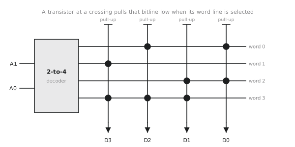
Take a BCD to seven-segment decoder: 4 inputs, 7 outputs. A $16 \times 7$ ROM holds the whole thing. Put 0111111 at address 0 for the digit 0, 0000110 at address 1 for the digit 1, and so on. No maps, no minimisation, no hazards. The cost is exponential in the inputs: 16 words for 4 inputs, 256 for 8, 65 536 for 16. Past about 20 inputs a ROM is out of the question and you go back to logic.
The technologies
Mask ROM has its contents fixed by one of the masks in fabrication: a transistor is present or not at each crossing. It is the densest and cheapest per bit at volume, unchangeable, and only worth the mask cost above something like a hundred thousand units. Game cartridges were mask ROM.
PROM ships blank and is programmed once by blowing fuses at selected crossings, with a programmer that applies a high current. It cannot be erased.
EPROM stores the bit as charge on a floating gate, a gate inside the oxide with no connection to anything. Programming injects charge with a high voltage; erasing means taking the chip out and putting it under an ultraviolet lamp for twenty minutes, through the quartz window on top. Reprogrammable, and a nuisance.
EEPROM erases electrically, by tunnelling the charge off the floating gate, in circuit and byte by byte. Writes are slow, milliseconds per byte, and the oxide wears out after $10^5$ to $10^6$ cycles. Microcontrollers include a few hundred bytes to a few kilobytes of it for calibration and settings.
Flash is EEPROM that erases in blocks, kilobytes at a time, which is what makes its density possible. NOR flash reads randomly at about 100 ns and is where a microcontroller’s program lives, executed in place. NAND flash is denser and cheaper, reads in pages, and is what SSDs, cards and USB sticks are made of. A modern NAND cell stores three or four bits by distinguishing eight or sixteen levels of charge, and trades endurance for that density.
The FPGA lookup table
An FPGA’s basic logic element is a lookup table, a LUT, with 4 or 6 inputs. A 4-input LUT is a $16 \times 1$ ROM whose contents are SRAM cells loaded from the configuration bitstream at power-up: sixteen bits of truth table and a 16-to-1 mux tree with the four inputs as the select (Figure 2).

There are $2^{16}$ functions of four variables and the LUT can be any of them, by loading the right sixteen bits. That is what programming an FPGA means. It is not a processor executing instructions; it is a large array of small ROMs and flip-flops, with programmable wiring between them, and the synthesis tool’s job is to cut your logic into pieces that fit in LUTs. A 6-input LUT is a $64 \times 1$ ROM.
Other uses
A sine table: address with the phase, read the amplitude. A numerically controlled oscillator is a phase accumulator, a counter with a programmable step, driving a sine ROM, and it is the core of direct digital synthesis. A character generator: address with the character code and the scan line, read a row of pixels. Code conversion, BCD to binary, Gray to binary, error-correction syndromes: any mapping from one code to another with no algebraic structure is a ROM.
| Inputs | ROM size per output bit | Choice |
|---|---|---|
| up to 4 | 16 | a LUT on an FPGA; gates on an ASIC |
| 5 to 8 | 32 to 256 | ROM for irregular functions, logic for structured ones |
| 9 to 16 | 512 to 65 536 | ROM only if the function has no structure |
| over 20 | over a million | logic, pipelined if necessary |
A 32-bit adder has 64 inputs and would need a $2^{64}$-entry ROM, but it has structure and an adder circuit is small. An arbitrary 10-input, 8-output code mapping has no structure and is a $1024 \times 8$ ROM.
Module 3 in review
Latches and flip-flops. Two inverters in a loop hold a bit. Adding control inputs gives the SR latch, then the D latch, which is transparent while enabled, and two D latches back to back give the edge-triggered flip-flop. Setup, hold and clock-to-Q are the three numbers that define it.
Synchronous design. One clock, every flip-flop on it, and all timing reduces to one inequality per path. Asynchronous inputs go through synchronisers because metastability cannot be prevented, only made rare.
State machines. State diagram, state table, encoding, excitation equations, circuit, and the same procedure in Verilog. Moore outputs from state alone, Mealy from state and input.
Registers and counters. A register is flip-flops with a shared enable. Shift registers turn serial into parallel and back, and with feedback become ring counters, Johnson counters and LFSRs. A counter is an adder with one operand fixed at 1, and a modulo-N counter clears on $N-1$.
Memory. A register file is a decoder, an array of registers and a mux per read port. SRAM stores a bit in a six-transistor latch, DRAM in a capacitor that must be refreshed, ROM in the presence or absence of a transistor. A LUT is a ROM used as logic.
Everything in this module was built from gates and flip-flops by hand. Module 4 introduces Verilog, and the reason for doing it this way first is that the language describes exactly these circuits. When you write an always @(posedge clk) block you should see the flip-flops; when you write count + 1 you should see the carry chain.
Practice Exercise
Problem 1. A sine generator uses a 10-bit phase accumulator as the ROM address and 12-bit amplitudes. How many entries, how many bits, and what output frequency does a step of 1 give at 100 MHz?
Solution
$2^{10} = 1024$ entries of 12 bits, 12 288 bits. With a step of 1 the accumulator takes 1024 cycles per revolution, so $100,\text{MHz} / 1024 = 97.66,\text{kHz}$. For a step $k$ the frequency is $k \times 97.66$ kHz; that is a numerically controlled oscillator.
Problem 2. Show that $F(A, B, C, D) = AB \oplus C\overline{D}$ fits in one 4-input LUT and give the sixteen configuration bits.
Solution
Every function of four variables fits. Enumerate ABCD from 0000 to 1111: $AB$ is 1 for 1100 to 1111, $C\overline{D}$ is 1 for 0010, 0110, 1010, 1110, and F is their XOR:
| ABCD | F | ABCD | F |
|---|---|---|---|
| 0000 | 0 | 1000 | 0 |
| 0001 | 0 | 1001 | 0 |
| 0010 | 1 | 1010 | 1 |
| 0011 | 0 | 1011 | 0 |
| 0100 | 0 | 1100 | 1 |
| 0101 | 0 | 1101 | 1 |
| 0110 | 1 | 1110 | 0 |
| 0111 | 0 | 1111 | 1 |
With address 0 at the least significant bit, the configuration word is $1011,0100,0100,0100$, or 0xB444. The synthesis tool computes a word like this for every LUT in the design.
Problem 3. A 12-input, 8-output mapping with no structure is needed on an FPGA. How big is the ROM, and should it be built from LUTs?
Solution
$2^{12} \times 8 = 32,768$ bits, 4 KB. Built from 4-input LUTs, each output bit is a 12-input function and needs a tree of a few dozen LUTs, several hundred in all, most of whose area is mux trees rather than storage. The right answer is the FPGA’s block RAM, a dedicated SRAM macro that holds the table directly and reads it in one cycle. LUTs are for logic; tables of more than a few hundred bits go in block RAM.
That completes the hardware half of the course. Module 4 begins with the question of why anyone would want to describe a circuit in text at all, and what a hardware description language is and is not.