The SR Latch
In the last article two cross-coupled inverters gave us two stable states, but no way to choose between them except by forcing the nodes from outside. In this article we replace the inverters with NAND gates. A NAND gate with one input held low outputs 1 whatever its other input does, which is exactly the override we need; with that input high it behaves as an inverter and the feedback works as before. The result is the SR latch, the first memory element with proper controls, and the ancestor of every flip-flop.
The circuit
Two NAND gates, each output feeding one input of the other (Figure 1).
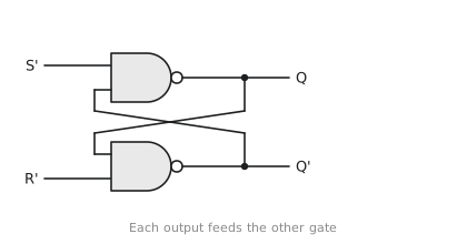
The upper gate takes $\bar{S}$ and $\bar{Q}$ and produces $Q$; the lower takes $\bar{R}$ and $Q$ and produces $\bar{Q}$. The inputs are written with bars because they are active low: to set the latch you pull $\bar{S}$ to 0. That is a consequence of building it from NANDs. In normal operation $Q$ and $\bar{Q}$ are complements.
The four input conditions
| $\bar{S}$ | $\bar{R}$ | $Q$ | $\bar{Q}$ | |
|---|---|---|---|---|
| 0 | 1 | 1 | 0 | set |
| 1 | 0 | 0 | 1 | reset |
| 1 | 1 | previous | previous | hold |
| 0 | 0 | 1 | 1 | forbidden |
Set. $\bar{S} = 0$ forces the upper NAND’s output to 1, so $Q = 1$. The lower NAND now has $\bar{R} = 1$ and $Q = 1$, both high, so $\bar{Q} = 0$. That feeds back to the upper gate, but with $\bar{S} = 0$ its output stays 1 regardless. Stable at $Q = 1$.
Reset. The mirror image: $\bar{R} = 0$ forces $\bar{Q} = 1$, then the upper gate sees two highs and gives $Q = 0$.
Hold. With both inputs at 1, both gates act as inverters and the circuit is the cross-coupled pair from the last article. It keeps whatever state it was in.
Forbidden. With both inputs at 0, both outputs are forced to 1. $Q$ and $\bar{Q}$ are no longer complements and the latch is not holding a valid state.
The forbidden state is worse than “not useful”. The problem is leaving it. If both inputs go back to 1 together, both gates try to pull their outputs low at once, and whichever wins decides the final state. That depends on which transistor happens to be a little faster, on temperature, on supply voltage. The result is unpredictable. In a real design, arriving at $\bar{S} = \bar{R} = 0$ is a bug.
The NOR version
The same latch can be built from two NOR gates, with active-high inputs: the upper NOR takes $S$ and $\bar{Q}$ and gives $Q$, the lower takes $R$ and $Q$ and gives $\bar{Q}$.
| $S$ | $R$ | $Q$ | $\bar{Q}$ | |
|---|---|---|---|---|
| 0 | 0 | previous | previous | hold |
| 1 | 0 | 1 | 0 | set |
| 0 | 1 | 0 | 1 | reset |
| 1 | 1 | 0 | 0 | forbidden |
Everything is inverted relative to the NAND version: hold is 00 instead of 11 and the forbidden state drives both outputs low instead of high. In CMOS the NAND gate is the faster of the two, for the reason we saw in Module 1, so the NAND latch is the more common.
Timing
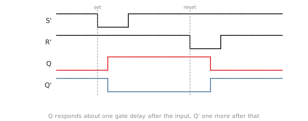
The SR latch has no clock. It responds to its inputs as soon as they change, limited only by gate delay. When $\bar{S}$ goes low, $Q$ rises one NAND delay later, and $\bar{Q}$ falls one more NAND delay after that (Figure 2). This immediate response is what makes it a latch rather than a flip-flop.
Debouncing a switch
A mechanical switch does not close cleanly. The contacts bounce for several milliseconds, opening and closing five or ten times before they settle, and each bounce looks like a separate press to a circuit that is counting presses.
A single-pole double-throw switch and an SR latch solve this with no software and no timer. The common terminal is grounded, and the two other terminals go to $\bar{S}$ and $\bar{R}$, each with a pull-up resistor. Moving the switch to the set side pulls $\bar{S}$ low on the first contact and $Q$ goes high. The following bounces take $\bar{S}$ high again, but that is only the hold condition, and $Q$ stays high. The output sees one clean edge (Figure 3). The same happens on the way back through $\bar{R}$.
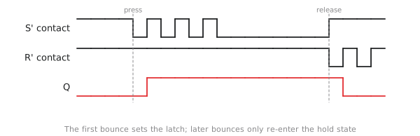
This works because the bounces never reach the opposite terminal: a contact that has bounced open is not touching the other side. The circuit is in keyboards and control panels everywhere.
Practice Exercise
Problem 1. An SR latch starts at $Q = 0$. The inputs $(\bar{S}, \bar{R})$ go through $(1,1)$, $(0,1)$, $(1,1)$, $(1,0)$, $(1,1)$. Trace $Q$.
Solution
$(1,1)$ hold, $Q = 0$. $(0,1)$ set, $Q = 1$. $(1,1)$ hold, $Q = 1$. $(1,0)$ reset, $Q = 0$. $(1,1)$ hold, $Q = 0$.
Problem 2. A NAND latch is in the forbidden state and both inputs are released to 1 at the same moment. Why is the result unpredictable?
Solution
At the moment of release both outputs are 1 and both gates see two high inputs, so both want to go low. If the upper gate gets there first, $Q = 0$ forces $\bar{Q} = 1$, which keeps $Q$ at 0: the reset state. If the lower gate is first, the latch ends up set. Which gate wins depends on sub-nanosecond differences that nothing controls.
Problem 3. Design a set-dominant latch, where asserting both set and reset gives $Q = 1$.
Solution
Block reset while set is active: in active-high terms, feed the latch $R_{eff} = R \cdot \bar{S}$ instead of $R$. Then $S = R = 1$ gives $R_{eff} = 0$ and the latch sets. The characteristic equation is $Q_{next} = S + \bar{R}Q$. The reset-dominant version is $Q_{next} = \bar{R}(S + Q)$.
The SR latch’s awkwardness is that you have to manage two inputs and never assert both. In the next article one extra gate removes the forbidden state and gives us a latch that stores whatever is on a single data wire.