The Synchronous Design Discipline
The first article of this section sketched the synchronous contract. This one spells it out as six rules. None of them is a convention for its own sake; each one exists because breaking it produces a particular kind of failure, and if you know the failure you can recognise the violation whatever form it takes.
Rule 1: all state lives in flip-flops on one clock
Every bit the circuit keeps from one cycle to the next is in a D flip-flop. Not a latch, not a cross-coupled pair of gates, not the charge on a wire. A flip-flop’s behaviour is exactly specified: Q changes at the edge, from what D was in the setup window, and holds otherwise. That is what timing analysis is built on.
A transparent latch breaks it, because while its enable is high its output is combinational, and any hold analysis downstream has to consider the whole enable window rather than one edge. The tools can handle latches, but it is harder and easier to get wrong, so use flip-flops.
The “one clock” part is what keeps analysis tractable. Flip-flops on different clocks have no defined timing relationship until you declare one. A design with undeclared clocks passes timing analysis with wrong answers.
Rule 2: combinational logic sits between registers
The shape of a synchronous design is registers separated by clouds of combinational logic (Figure 1). The path from one Q to the next D is a pure function with a bounded delay, and static timing analysis measures the longest such path and compares it with the period.
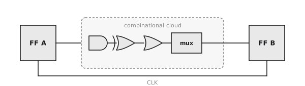
The rule is broken by anything with state inside the cloud: a latch, a tri-state conflict, or, worst of all, a loop.
Rule 3: no combinational feedback loops
A combinational loop is a path from a node back to itself without a flip-flop in it. This is the most dangerous violation there is.
// do not do this
assign carry_out = (a & b) | (carry_out & (a ^ b));
carry_out appears on both sides. A zero-delay simulator will usually converge on some value and say nothing. In silicon the behaviour depends on the loop’s delay: for some inputs it settles, for others it oscillates at a frequency of about $1 / (2 t_{loop})$, hundreds of megahertz or more, corrupting anything nearby and burning power. When synthesis says “combinational loop detected”, it is reporting a bug, not a warning to acknowledge. The fix is a flip-flop in the loop.
Rule 4: synchronise every input from outside the domain
Anything that originates outside the clock domain, another domain, a pin, a test input, is asynchronous to the local clock. Connected directly to a D input it can change inside the setup or hold window, and the flip-flop can go metastable. A metastable output that reaches other flip-flops before it resolves corrupts state in ways you cannot see from outside.
The remedy is a synchroniser, two flip-flops in series, which does not prevent metastability but gives it a full clock period to resolve before anything uses the result. The last article in this section covers it.
Rule 5: manage resets carefully
A reset puts the design into a known state. There are two families.
A synchronous reset is data:
always_ff @(posedge clk) begin
    if (rst)
        q <= 1'b0;
    else
        q <= d;
end
It takes effect at the next edge, timing analysis treats it as any other path, and it needs the clock to be running.
An asynchronous reset acts immediately:
always_ff @(posedge clk or negedge rst_n) begin
    if (!rst_n)
        q <= 1'b0;
    else
        q <= d;
end
Asserting it is safe at any time. Releasing it is not: the release happens at an arbitrary time relative to the clock, and if it falls in the setup-hold window the flip-flop can go metastable on its first cycle of normal operation.
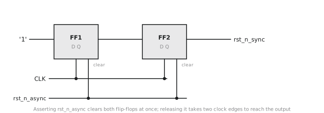
Standard practice combines the two: assert asynchronously, release synchronously, through the circuit in Figure 2. Two flip-flops with their D chain tied to 1 are cleared by the raw reset. When the raw reset releases, a 1 propagates through them on successive clock edges, and the output reset releases on an edge.
Rule 6: no gated clocks without proper cells
Clock gating saves power, and done wrongly it produces the worst kind of bug, a spurious clock edge that captures garbage.
// wrong: raw AND gate in the clock path
wire gated_clk = clk & (count == 8'd255);

always_ff @(posedge gated_clk)
    snapshot <= data;
The comparator is combinational and glitches as the bits of count settle. The AND gate passes every glitch to the flip-flop as a clock edge, and the flip-flop samples data at random moments. It works in zero-delay simulation and fails in silicon, at some temperatures and not others.
If the intent is “capture when count reaches 255”, the clock should not be touched at all:
always_ff @(posedge clk)
    if (count == 8'd255)
        snapshot <= data;
If the goal really is to save clock power on a large register bank, use a clock-gating cell with a registered enable:
logic enable_reg;
always_ff @(posedge clk)
    enable_reg <= (count == 8'd254);   // true one cycle early

ICG icg_inst (.CK(clk), .EN(enable_reg), .GCLK(gated_clk));

always_ff @(posedge gated_clk)
    snapshot <= data;
The cell’s latch takes the enable on the low phase and holds it through the rising edge, so the gated clock is just the clock with some pulses missing.
An example violation
A designer wants a priority encoder that remembers the last grant when there are no requests:
module priority_tracker (
    input  logic [3:0] req,
    output logic [1:0] grant
);
    logic [1:0] last_grant;

    always_comb begin
        casez (req)
            4'b1???: grant = 2'd3;
            4'b01??: grant = 2'd2;
            4'b001?: grant = 2'd1;
            default: grant = last_grant;   // uses last_grant
        endcase
    end

    assign last_grant = grant;   // and last_grant is grant
endmodule
That is a loop: req to grant to last_grant to grant. With req at zero the circuit tries to hold grant through combinational feedback, and whether it holds or oscillates depends on delays. The fix is to register the fallback:
module priority_tracker (
    input  logic       clk,
    input  logic       rst_n,
    input  logic [3:0] req,
    output logic [1:0] grant
);
    logic [1:0] last_grant_reg;

    always_ff @(posedge clk or negedge rst_n) begin
        if (!rst_n)
            last_grant_reg <= 2'd0;
        else
            last_grant_reg <= grant;
    end

    always_comb begin
        casez (req)
            4'b1???: grant = 2'd3;
            4'b01??: grant = 2'd2;
            4'b001?: grant = 2'd1;
            default: grant = last_grant_reg;
        endcase
    end
endmodule
The fallback is now one cycle old, which is what the designer meant anyway, and the circuit can be analysed.
The six rules
| Rule | Requirement | What breaking it causes |
|---|---|---|
| 1 | state in clocked flip-flops | untimed state, meaningless timing analysis |
| 2 | combinational logic between registers | the same |
| 3 | no combinational loops | oscillation, corrupted state |
| 4 | synchronise external inputs | metastability spreading through the design |
| 5 | manage resets | wrong initial state, metastability on release |
| 6 | gating cells for gated clocks | spurious clock edges |
A design that keeps all six is one in which every flip-flop captures a timing-verified value at every edge and does nothing at any other time.
Practice Exercise
Problem 1. Synthesis reports “inferred latch for signal state[1] in always_comb”. Is that a violation, what causes it, and what is the fix?
Solution
Rule 1. The usual cause is an always_comb block that does not assign the signal on every path, typically a case statement with a missing branch:
always_comb begin
    case (sel)
        2'b00: state = 4'b0001;
        2'b01: state = 4'b0010;
        2'b10: state = 4'b0100;
        // 2'b11 missing
    endcase
end
For the missing input the tool has to hold the old value, so it infers a latch. Assign a default before the case, or cover every branch:
always_comb begin
    state = 4'b0000;
    case (sel)
        2'b00: state = 4'b0001;
        2'b01: state = 4'b0010;
        2'b10: state = 4'b0100;
        2'b11: state = 4'b1000;
    endcase
end
Problem 2. A board-level supervisor releases reset asynchronously. Write the reset synchroniser and say why it needs two stages.
Solution
module reset_synchronizer (
    input  logic clk,
    input  logic rst_n_async,
    output logic rst_n_sync
);
    logic ff1_q, ff2_q;

    always_ff @(posedge clk or negedge rst_n_async)
        if (!rst_n_async) ff1_q <= 1'b0;
        else              ff1_q <= 1'b1;

    always_ff @(posedge clk or negedge rst_n_async)
        if (!rst_n_async) ff2_q <= 1'b0;
        else              ff2_q <= ff1_q;

    assign rst_n_sync = ff2_q;
endmodule
The first flip-flop may go metastable if the release lands near an edge; the second gives it a full period to resolve before its output is used. Every flip-flop in the design takes its asynchronous clear from the raw reset, so assertion is immediate, and its normal operation resumes on the synchronised release.
Problem 3. Why is wire gated_clk = clk & en_reg; still wrong when en_reg is a flip-flop output?
Solution
en_reg changes a clock-to-Q after a rising edge, while the clock is high. As it rises, the AND output rises with it, a clock edge in the wrong place; as it falls, the AND output falls, a truncated pulse. A gating cell captures the enable on the low phase precisely so that it is stable before the clock rises.
The next article looks at what actually goes wrong when these rules are not followed: races, essential hazards, and the reset release problem.