DRAM and the Memory Hierarchy
SRAM stores a bit in six transistors. A 16 GB main memory built that way would need about $16 \times 2^{30} \times 8 \times 6 \approx 8 \times 10^{11}$ transistors, which is not going to happen. DRAM stores a bit in one transistor and one capacitor, and this article is about what that costs.
The cell
An NMOS access transistor, gate on the word line, connects a small capacitor to the bitline (Figure 1). Charge on the capacitor is a 1, no charge is a 0. The capacitor is about 20 to 30 fF in a modern process and is built as a deep trench or a tall stack, because there is no room for it beside the transistor.
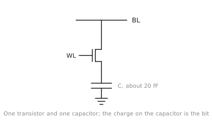
There is nothing holding the charge in place except the off-state of the transistor and the dielectric of the capacitor, and both leak. At room temperature a cell is unreadable within a few tens of milliseconds. So every cell has to be read and rewritten, refreshed, more often than that, forever, for as long as the data is to survive.
Reading
The bitline is precharged to $V_{DD}/2$. The word line rises and the cell capacitor shares its charge with the bitline:
$$V_{BL} = \frac{V_{DD}}{2} + \frac{C_s}{C_s + C_{BL}} \left( V_{cell} - \frac{V_{DD}}{2} \right)$$
The bitline is long and its capacitance is around ten times the cell’s, so the bitline moves by only 50 to 100 mV, up for a stored 1 and down for a 0. A sense amplifier compares it with a reference bitline held at $V_{DD}/2$ and amplifies the difference to full rail.
Sharing the charge with the bitline has destroyed it: the cell now holds a voltage close to $V_{DD}/2$, which is neither value. So the sense amplifier is left connected, with the word line still high, until the bitline at full rail has recharged the capacitor to its original value. Only then does the word line drop. Every DRAM read is a read followed by a write-back, and that alone makes it slower than SRAM.
Writing is simpler. Drive the bitline to the value, raise the word line, wait for the capacitor to charge or discharge through the transistor, drop the word line.
Refresh
A DDR4 device has to refresh every row within 64 ms. The controller issues a refresh command every 7.8 µs, each of which refreshes a group of rows, and while a bank is refreshing it cannot serve reads or writes. A few per cent of the bandwidth goes to refresh, more at high temperature, where leakage is worse and the interval is halved to 32 ms. The 64 ms is a guarantee for the worst cell in the array; most cells would hold their charge far longer.
The row buffer
When a word line rises, every cell in that row, several kilobytes of them, is sensed at once, and their values sit in the sense amplifiers. That row of sense amplifiers is the row buffer (Figure 2), and while a row is open, any column in it can be read with a column address alone.
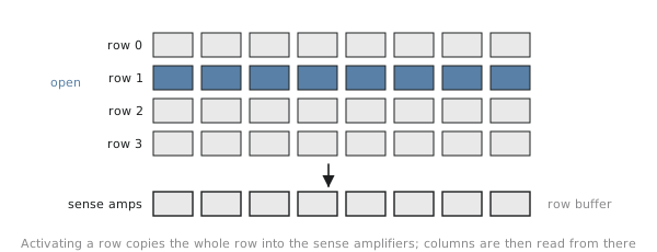
That gives three cases. A row hit, where the wanted row is already open, costs only the column access, CL, about 14 ns. A row miss with nothing open costs an activate, $t_{RCD}$, plus CL. A row conflict, where a different row is open, costs a precharge to close it, $t_{RP}$, then the activate, then the column access, 40 to 60 ns before the first data appears (Figure 3). The controller reorders requests to make row hits common, and this is why sequential access is so much faster than random access to DRAM.
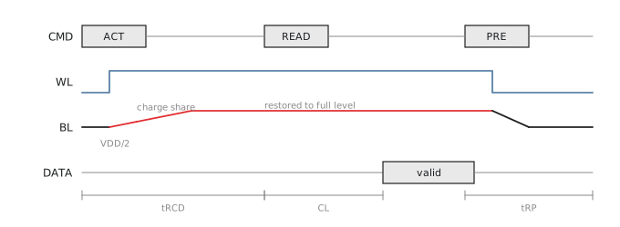
For DDR4-3200, $t_{RCD}$, CL and $t_{RP}$ are each about 14 ns, and the minimum time a row must stay open, $t_{RAS}$, about 32 ns. These numbers have barely moved in fifteen years. What has moved is bandwidth.
Bandwidth against latency
Double data rate transfers a word on both clock edges. DDR4-3200 moves 3200 million transfers a second on a 64-bit bus:
$$3200 \times 10^6 \times 8,\text{bytes} = 25.6,\text{GB/s}$$
DDR5-6400 doubles that per channel, and two channels double it again. But the first byte of a random access still takes 60 to 80 ns, about what DDR3 took. Bandwidth comes from parallelism, more banks and wider prefetch; latency comes from the physics of a long bitline and a small capacitor, and that does not improve much.
The hierarchy
| Level | Technology | Capacity | Latency | Cycles at 3 GHz |
|---|---|---|---|---|
| Registers | flip-flops | a few hundred bytes | under 0.1 ns | 0 |
| L1 | SRAM | 32 to 64 KB | about 1 ns | 3 to 4 |
| L2 | SRAM | 256 KB to 4 MB | about 5 ns | 12 to 15 |
| L3 | SRAM | 8 to 64 MB | about 20 ns | 40 to 60 |
| Main memory | DRAM | 8 to 256 GB | about 80 ns | 200 to 250 |
| SSD | NAND flash | 256 GB to 8 TB | about 100 µs | 300 000 |
| Hard disk | magnetic | 1 to 20 TB | about 10 ms | 30 million |
Each level is several times bigger and several times slower than the one above, and the scheme works because programs reuse data they used recently and data near it. A processor waiting 250 cycles for every load would be idle almost all the time; with good hit rates in the caches it almost never waits that long, and most of computer architecture since the 1990s is the effort to keep it that way.
Practice Exercise
Problem 1. A cell stores 0. The bitline is precharged to 0.6 V, the cell capacitance is 25 fF and the bitline capacitance 250 fF. What is the bitline voltage after charge sharing?
Solution
$$V_{BL} = 0.6 + \frac{25}{275}(0 - 0.6) = 0.6 - 0.0545 = 0.545,\text{V}$$
The bitline falls by 55 mV. The sense amplifier has to resolve that against a 0.6 V reference, which is why it is a regenerative circuit and not a plain comparator.
Problem 2. A device has 65 536 rows to be refreshed every 64 ms, one row per refresh command, and each refresh occupies the bank for 55 ns. How often must the controller refresh, and what fraction of the time is the bank busy with it?
Solution
$64,\text{ms} / 65,536 = 976,\text{ns}$ between refreshes. $55 / 976 \approx 5.6,%$ of the time.
Problem 3. L1 hits 90 % of accesses, L2 hits 80 % of what misses L1, L3 hits 90 % of what misses L2, with latencies 1, 5, 20 and 80 ns. What is the average memory access time?
Solution
Working from the bottom: L3 and below is $20 + 0.1 \times 80 = 28$ ns. L2 and below is $5 + 0.2 \times 28 = 10.6$ ns. Overall, $1 + 0.1 \times 10.6 = 2.06$ ns. With those hit rates the processor sees close to L1 latency even though DRAM is eighty times slower.
SRAM and DRAM both forget when the power goes. The last article of the module is about memory that does not, and about a trick that turns memory into logic.