Register Files
A register holds one value. A processor needs a few dozen of them, and it needs to read two and write one in every cycle. This section is about memory, starting with the smallest kind, the register file, and going on to SRAM, DRAM and ROM.
What it looks like from outside
A register file has $N$ registers of $W$ bits. The processor reads its operands from it and writes its results back, so it needs at least two read ports and one write port, to run an instruction like ADD rd, rs1, rs2 in one cycle: read rs1 and rs2, add, write rd.
| Architecture | Registers | Width | Read ports | Write ports |
|---|---|---|---|---|
| RISC-V RV32I | 32 | 32 | 2 | 1 |
| ARM AArch64 | 31 plus SP | 64 | 2 | 1 |
| x87 FPU | 8 | 80 | 2 | 1 |
| AVX-512 | 32 | 512 | 2 | 1 |
Each read port has an address input and a data output. The write port has an address, a data input and a write enable. Everything is on one clock.
The write side
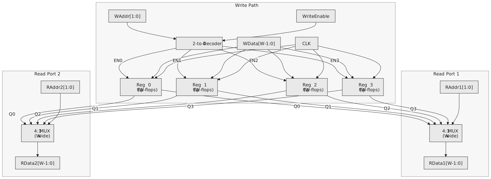
Every register is a $W$-bit register with a load enable, as in section 3.4. The write data bus goes to the D inputs of all of them in parallel. Which one loads is decided by a decoder on the write address, gated by the write enable:
$$WE_i = WriteEnable \cdot (WAddr = i)$$
With the enable low, nothing loads, whatever is on the address and data. With it high, exactly one register captures the data at the clock edge.
The read side
Reading is combinational. Each read port is a $W$-bit wide $N$-to-1 mux with the port’s address as the select:
$$RData_1 = Reg[RAddr_1] \qquad RData_2 = Reg[RAddr_2]$$
The two muxes are independent. Any number of ports can read the same register at once, and the data appears a mux delay after the address, with no clock involved. Figure 1 shows the whole thing for four registers.
In RISC-V register x0 always reads as zero. The cheapest way to get that is to leave register 0 out of the array and put a constant on that mux input.
Reading and writing the same register
If a read port and the write port carry the same address in the same cycle, what comes out? With the circuit above, the mux is connected to the register’s Q, and Q does not change until the edge at the end of the cycle, so the read sees the old value. This is read-before-write, and it is what most register files do. If you want the new value in the same cycle, add a comparator between the read and write addresses and a bypass mux that takes the write data instead of the register output when they match. Most designs keep the register file simple and do the bypass outside it, in the pipeline, where it is called forwarding.
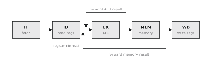
Consider two instructions back to back, the first writing x3 and the second reading it. In a five-stage pipeline the first writes x3 in its fifth stage, but the second reads the register file in its second stage, three cycles earlier, and gets the stale value. Forwarding fixes this with muxes in front of the ALU that take the result straight from the end of the execute or memory stage when the addresses match (Figure 2). The register file still does read-before-write; the pipeline routes around it.
What ports cost
Every read port is another $N$-to-1 mux, $W$ bits wide. Every write port is another decoder and another input to the mux in front of every flip-flop. The area grows roughly with $R \times W \times N$ for $R$ read ports. That is why two reads and one write is the norm. Out-of-order processors, which need to read and write several instructions’ worth of operands per cycle, have register files with 8 or more read ports and 4 or more write ports, over a hundred or more physical registers, and they are among the largest and hottest structures on the die.
A flip-flop register file is reasonable up to something like 64 or 128 entries. Beyond that the flip-flops and the muxes get too big and a custom SRAM macro takes over, usually with fewer ports per copy; a GPU register file with thousands of entries is SRAM. The next article is about that cell.
Practice Exercise
Problem 1. A register file has 32 registers of 32 bits, with 2 read ports and 1 write port. How wide is the write address, and how many flip-flops are there?
Solution
$\log_2 32 = 5$ address bits, plus the write enable. $32 \times 32 = 1024$ flip-flops, before the decoder and the two 32-to-1 muxes.
Problem 2. In the four-register file, the write enable is low but the write address and data are valid. What happens?
Solution
Every $WE_i$ is the AND of the write enable with a decoder output, so all four are 0. No register loads, and the address and data are ignored. That is the point of the enable.
Problem 3. In a five-stage pipeline, ADD x3, x1, x2 is followed immediately by ADD x5, x3, x4. The first writes x3 in stage 5; the second reads x3 in stage 2. Without forwarding, what does the second read? With forwarding from the execute stage, how is it fixed?
Solution
Without forwarding the second instruction reads the register file while the first is still in stage 3, so it gets whatever x3 held before, and computes the wrong sum. With forwarding, the hardware compares the first instruction’s destination with the second’s sources and, when they match and the first has its write enable set, the mux in front of the ALU takes the first instruction’s ALU output directly. The condition also excludes x0, which is never written.
The register file is flip-flops, and flip-flops are too big for kilobytes. The next article is about the six-transistor cell that every cache is made of.