Shift Register Applications
The last article gave the four forms of shift register. This one is about what they are used for, because the chain of flip-flops turns up in far more places than serial ports. Five applications follow, each showing a different side of it.
Delay lines
A serial-in, serial-out register of $N$ stages delays a signal by exactly $N$ clock periods. In a pipeline where one path takes three stages and a parallel path takes five, the shorter path needs two cycles of delay before the results can be combined, and a two-stage shift register is the exact tool. Video pipelines do this constantly to keep, say, luminance and chrominance lined up on the same pixel.
UART
A UART is the simplest serial link: two wires, no clock, and a bit rate both ends agree on in advance. A frame in the common 8N1 format is ten bits: a start bit (0), eight data bits least significant first, and a stop bit (1). The line idles high (Figure 1).

The transmitter is a PISO: load the byte, add the start and stop bits, and shift out at the bit rate. The receiver is a SIPO with a timing problem: it sees the falling edge of the start bit, waits half a bit period so as to sample in the middle of each bit, shifts in eight bits at the bit rate, checks for the stop bit, and raises data-valid. Because there is no transmitted clock, the receiver’s bit clock has to be within a couple of percent of the transmitter’s or the sampling point drifts off the bit.
Ring counters
Connect the last Q back to the first D and load a single 1. The 1 goes round the ring, one place per clock (Figure 2). A 4-bit ring counter has four states, 0001, 1000, 0100, 0010, and each output is high in exactly one of them.
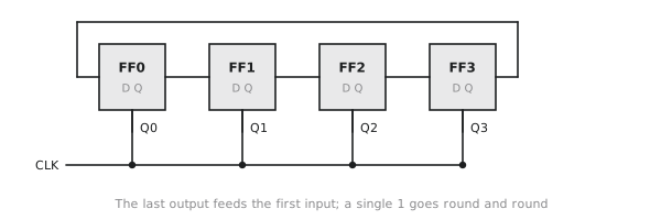
It is a one-hot sequencer with no decoding at all, used to step through phases, banks or enables in turn. Its weakness is that if the single 1 is ever lost, at power-up or by a soft error, the ring is all zeros for ever. Real designs reset it to a valid pattern and often add a detector that re-injects a 1 if the register is found empty.
Linear feedback shift registers
Feed the serial input from the XOR of some of the register’s own bits, the taps, and the register runs through a pseudo-random sequence. With the right taps an $N$-bit register visits all $2^N - 1$ non-zero states before repeating. Figure 3 shows a 4-bit example with taps at bits 3 and 2, the polynomial $x^4 + x^3 + 1$.
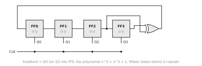
$$D[0] \leftarrow Q[3] \oplus Q[2], \qquad D[i] \leftarrow Q[i-1]$$
From 0001 the sequence runs 0010, 0100, 1000, 1001, 1011, 1111, 0111, 1110, 0110, 1101, 0101, 1010, 1100, 0011, and back to 0001: fifteen states, every non-zero value once. The all-zeros state is the one it can never reach, and the one it can never leave.
LFSRs are everywhere. A pseudo-random bit sequence for stressing a high-speed link is an LFSR output; PRBS-7 and PRBS-31 are standard test patterns. Built-in self-test blocks use an LFSR to generate test vectors on chip. And a cyclic redundancy check is an LFSR: computing a CRC is polynomial division in modulo-2 arithmetic, and a shift register with XOR taps at the generator polynomial’s terms does exactly that division. The CRC-32 on every Ethernet frame is a 32-bit LFSR with taps from the polynomial $x^{32} + x^{26} + x^{23} + x^{22} + x^{16} + x^{12} + x^{11} + x^{10} + x^8 + x^7 + x^5 + x^4 + x^2 + x + 1$. You will build one at some point.
Scan chains
A chip has millions of flip-flops and no way to probe them. To test it after manufacture, every flip-flop gets a mux on its D input that, when a scan-enable signal is high, takes its input from the previous flip-flop instead of from the logic. With scan enabled, all the flip-flops in the chip form one enormous shift register, or more usually a few thousand parallel ones. The tester shifts in a test pattern, drops scan-enable for one clock so that the logic runs for a cycle, raises it again and shifts the result out, and compares with what was expected.
You write ordinary RTL and the synthesis tool inserts the scan muxes. The cost is around ten to fifteen percent of area for the muxes and their wiring. It is why testability is a design concern from the start, and why some flip-flop styles and reset conventions are preferred in production flows.
Practice Exercise
Problem 1. A 4-bit LFSR uses the polynomial $x^4 + x + 1$, taps at bits 3 and 0. Trace eight states from 0001.
Solution
Feedback is $Q[3] \oplus Q[0]$ into bit 0. From 0001: feedback 1, next 0011? Careful: the new bit enters at bit 0 and the rest shift up. 0001 → feedback $0 \oplus 1 = 1$ → 0011; → $0 \oplus 1 = 1$ → 0111; → 1111; → $1 \oplus 1 = 0$ → 1110; → $1 \oplus 0 = 1$ → 1101; → $1 \oplus 1 = 0$ → 1010; → $1 \oplus 0 = 1$ → 0101; → $0 \oplus 1 = 1$ → 1011. Continue and all fifteen non-zero states appear; this polynomial is also maximal.
Problem 2. How long is one 8N1 frame at 9600 baud, and how many frames per second?
Solution
A bit is $1/9600 \approx 104,\mu\text{s}$, so ten bits are about 1.04 ms, and 960 frames, that is 960 bytes, go by per second. A kilobyte takes about a second.
Problem 3. A six-phase sequencer is built as a ring counter. How many flip-flops, what is the sequence, and what happens if it resets to all zeros?
Solution
Six flip-flops; 000001, 100000, 010000, 001000, 000100, 000010, and back. If it ever holds all zeros it stays there. The reset value must be 000001, not zero, and a NOR across the register can be used to re-insert a 1 if it is ever found empty.
The last article in this section combines hold, shift left, shift right and load into one register with a mode input, the universal shift register.