Clock Signals and How They Are Distributed
In the last article the clock was the timekeeper of the whole design. In this one we look at the clock as a signal: what it has to be, where it comes from, and the problem of getting one edge to millions of flip-flops at very nearly the same instant. If the clock reaches one flip-flop a few tens of picoseconds late, a path fails timing. If it is noisy, flip-flops go metastable. No other signal on the chip carries as much responsibility.
What a clock needs to be
The right frequency, held within a few hundred parts per million over temperature and voltage.
Close to a 50 percent duty cycle. Some structures use both phases, and an asymmetric clock takes margin from one of them.
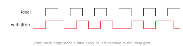
Low jitter. Jitter is the cycle-to-cycle wobble of the edge. If an edge can land 50 ps early or late, that 100 ps comes straight off the logic budget, because the edge no longer arrives at a known time but somewhere in a window (Figure 1).
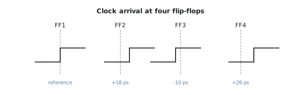
Low and uniform skew. Skew is the difference in the edge’s arrival time at different flip-flops (Figure 2). If a launching flip-flop sees the edge 200 ps before the capturing one, the path between them effectively has 200 ps less than a period. At 1 GHz that is a fifth of the budget.
Clean edges. A slow-slewing edge sits in the linear region of the gates it drives for too long, which costs power and invites noise.
Where the clock comes from
The crystal. A quartz crystal resonates mechanically at a frequency set by its dimensions, and that resonance is extremely stable: an ordinary crystal oscillator drifts under 50 ppm, and an oven-controlled one under 0.01 ppm. The board carries a crystal oscillator at some modest frequency, 25 MHz or 100 MHz, and feeds it to the chip on a clock pin.
The PLL. 25 MHz is far too slow for a processor at 3 GHz. A phase-locked loop multiplies the reference up. It is a feedback loop: a phase detector compares the reference with a divided-down copy of the output, a loop filter smooths the error into a control voltage, a voltage-controlled oscillator runs at a frequency set by that voltage, and a divider feeds the output back. When locked,
$$f_{out} = \frac{N}{M} f_{ref}$$
for divider ratios $N$ and $M$, so nearly any rational multiple of the reference is available. Every chip has at least one PLL, and lock takes microseconds to milliseconds after power-up.
The ring oscillator. An odd number of inverters in a ring oscillates at a frequency set by their delay. It is tiny and starts instantly, but its frequency wanders by 20 or 30 percent with process, voltage and temperature. It is used where precision does not matter, in random number generators, spread-spectrum clocking and process monitors, never for a system clock.
The distribution problem
Now take the PLL output, a 3 GHz clock with a few picoseconds of jitter, and deliver it to fifty million flip-flops over a die twenty millimetres across. The wires have resistance and capacitance, every branch adds delay, and different paths to different flip-flops have different delays. Left alone, the skew would swallow the budget.
Skew affects both constraints. If the capturing flip-flop’s clock arrives late relative to the launching one, the data has less time and setup suffers. If it arrives early, the launching flip-flop’s new data can reach the capturing one before its edge has passed, and hold suffers. Hold violations are the dangerous case, because they fail on every chip at every frequency, and fixing one after tape-out means a mask change.
Clock tree synthesis
The place-and-route flow has a dedicated step, clock tree synthesis, that finds every clock sink, builds a tree of buffers from the source to all of them, and inserts and sizes buffers so that the delay along every branch is as equal as it can be. The target is a few tens of picoseconds of skew across the die.
The ideal shape is the H-tree (Figure 3): a recursive H whose every leaf is the same wire length from the root, so that wire delay is the same to every flip-flop.
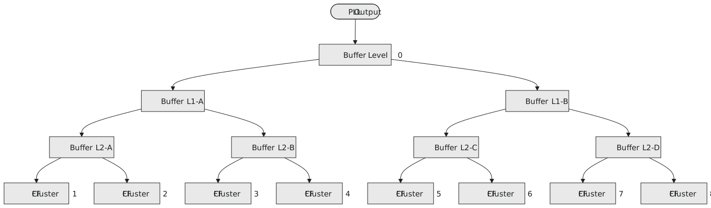
Real designs are not regular grids, so the tool starts from something like an H-tree and then balances the branches by adjusting buffer sizes and positions until the skew report is acceptable. On a large chip each core has its own tree with millions of endpoints and thousands of buffers, and the synthesis run takes hours. The clock tree is also where a large share of the chip’s dynamic power goes, commonly quoted as 20 to 40 percent, because every buffer switches every cycle.
Clock domains
A clock domain is the set of flip-flops that share one clock. Within it, timing analysis can guarantee setup and hold everywhere. A chip usually has several: the processor at one frequency, the GPU at another, a memory interface phase-locked to the memory clock, an I/O block on its own oscillator. A signal passing from one domain to another crosses a clock domain crossing, where setup and hold cannot be guaranteed because the two clocks have no fixed relationship. Every such signal has to be synchronised, and the last article in this section is about that.
Clock gating
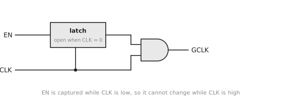
Because the clock tree burns power whether or not anything is happening, designs stop the clock to blocks that are idle. The naive way, an AND gate between the clock and an enable, is wrong: the enable is combinational, it glitches while it settles, and each glitch is a clock edge. The right way is an integrated clock-gating cell (Figure 4). It contains a latch that is open only while the clock is low, so the enable is captured before the clock rises and cannot change during the high phase, and the AND gate after it produces a clean gated clock.
Synthesis tools infer these cells from the ordinary enable pattern:
always_ff @(posedge clk) begin
    if (enable)
        q <= d;
end
The tool sees that q only changes when enable is set and can replace the mux on D with a gating cell on the clock for a whole bank of registers, saving power at no cost in area.
Practice Exercise
Problem 1. A clock tree has 40 ps of skew either way (80 ps between the worst pair), the period is 1 ns, setup is 80 ps and clock-to-Q is 120 ps. How much logic delay fits on a path between two flip-flops in the worst case?
Solution
Setup is worst when the launching clock is late and the capturing clock is early, an 80 ps penalty: $1000 - 80 - 120 - 80 = 720$ ps. Skew alone took 8 percent of the period.
Problem 2. A PLL has a 100 MHz reference, $N = 30$ and $M = 1$. What is the output, and is it valid if the VCO tunes from 2.5 to 3.5 GHz?
Solution
3 GHz, inside the VCO’s range, so the loop locks. $N = 35$ would give 3.5 GHz; 2.4 GHz is outside the VCO’s range and cannot be had by changing the dividers.
Problem 3. Is wire gated_clk = clk & enable_reg; acceptable if enable_reg is a flip-flop output?
Solution
No. When enable_reg changes, it does so a clock-to-Q after a rising edge, while the clock is high, and the AND output follows it: a misplaced rising edge or a truncated pulse. Timing analysis also cannot treat a clock derived from data properly. Use the enable in the D path and let synthesis infer a gating cell, or instantiate a clock-gating cell from the library.
The next article collects the rules of synchronous design into a discipline, with the failure that each rule prevents.