SRAM
A register file of flip-flops is fine up to a few hundred bits. A cache needs hundreds of kilobytes, and the cell that makes that possible is the six-transistor SRAM cell.
Why it exists
A processor at 3 GHz issues an instruction every 0.33 ns. A DRAM access takes on the order of 100 ns. If every load had to go to DRAM the processor would spend nearly all its time waiting, so between the two sits a hierarchy of caches, and every one of them is static RAM: static because it holds its data as long as power is on, with no refreshing, and random access because any location takes the same time. On-chip SRAM has access times from under a nanosecond to a couple of nanoseconds, which is close enough to the clock to be useful.
The cell
Four transistors make two cross-coupled inverters, the same bistable pair as the SR latch in section 3.1. M1 and M2 are one inverter with output Q; M3 and M4 are the other with output QB. Q drives the input of the second inverter and QB drives the input of the first, so the pair has two stable states and holds either one indefinitely (Figure 1).
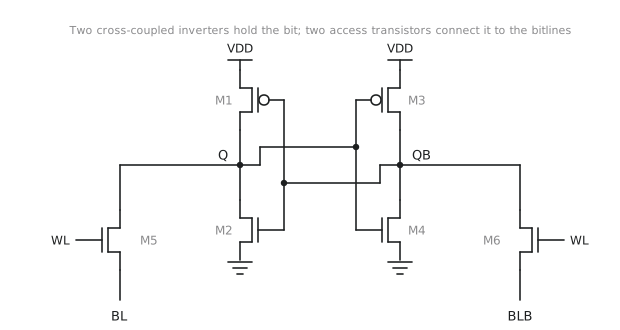
The other two transistors, M5 and M6, connect Q and QB to a pair of bitlines, BL and BLB, and their gates are on the word line. With the word line low the cell is isolated and just holds. With it high the cell is connected to the bitlines and can be read or written.
Reading
Both bitlines are first precharged to VDD. Then the word line goes high. Suppose the cell holds Q = 0, so QB = 1 and M2, whose gate is QB, is on. BL is now connected through M5 and M2 to ground and starts to fall. On the other side M4’s gate is Q = 0, so M4 is off and BLB stays up. A small difference opens between the two bitlines, a hundred millivolts or so, and a sense amplifier, a cross-coupled pair much like the cell itself, amplifies that difference to a full logic level (Figure 2). The word line drops, the cell is isolated again, and the bitlines are precharged for the next access.
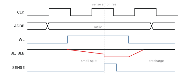
The cell is deliberately weak, so that it moves the bitline slowly and the bitline does not disturb it, and the read leaves the stored value unchanged. That is a non-destructive read, and it is one of the things that separates SRAM from DRAM.
Writing
To write, the write driver pulls one bitline all the way to ground, BL for a 0 and BLB for a 1, and leaves the other at VDD. Then the word line goes high. Now the bitline is fighting the cell’s own inverter for control of the storage node. The write driver is made stronger than the cell’s pull-up transistors, so it wins, the node is dragged over, the other inverter follows, and the cell flips. The word line drops and the cell holds the new value. The sizing matters: the access transistors have to be strong enough, relative to the pull-ups, for a write to succeed, and weak enough, relative to the pull-downs, for a read not to flip the cell. Those two ratios are the whole art of SRAM cell design.
The array
Cells go in a rectangular array (Figure 3). A row decoder takes the upper address bits and raises one word line, which connects a whole row of cells to their bitline pairs. Each column has its own sense amplifier and write driver at the bottom, shared by every row. A column mux on the lower address bits picks which columns go to the output; for an 8-bit output, eight columns at a time.
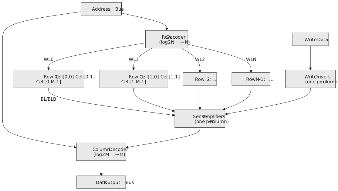
The access time, address to data, is the sum of the decoder, the word line rising, the bitline split and the sense amplifier. The cycle time is longer, because the bitlines have to be precharged before the next access. On-chip SRAM in a modern process has an access time around a nanosecond for a small array and several nanoseconds for a large one, which is why caches are split into levels.
In the hierarchy
| Level | Typical size | Access time | Cell | Cycles at 3 GHz |
|---|---|---|---|---|
| L1 (data and instruction) | 32 to 64 KB each | about 1 ns | fast, larger transistors | 3 to 4 |
| L2 | 256 KB to 4 MB | about 5 ns | balanced | 12 to 15 |
| L3 | 8 to 64 MB | about 20 ns | high density | 40 to 60 |
The L1 cache uses cells sized for speed; the L3 uses the smallest cell the process offers, because its area matters more than its latency. A desktop processor with 32 MB of L3 has about $32 \times 2^{20} \times 8 \times 6 \approx 1.6$ billion transistors in that one cache.
Practice Exercise
Problem 1. The cell holds Q = 1. The word line rises for a read. Which bitline falls, and why does the cell keep its value?
Solution
Q = 1 means QB = 0. M2’s gate is QB, so M2 is off and BL has no path to ground; it stays at VDD. M4’s gate is Q, so M4 is on and BLB discharges through M6 and M4. BLB falls, the sense amplifier sees BL above BLB and reports a 1. The current through M6 and M4 is small and the cross-coupled inverters hold Q at 1 throughout, because the access transistor is weaker than the pull-down.
Problem 2. An array has 1024 rows and 64 columns of single-bit cells with an 8-bit data bus. What is the capacity, and how wide are the row and column addresses?
Solution
$1024 \times 64 = 65,536$ bits, 8 KB. Row address $\log_2 1024 = 10$ bits. The 64 columns form 8 groups of 8, so the column address is 3 bits, and the total address is 13 bits for $2^{13} = 8192$ bytes.
Problem 3. Why must the write driver be stronger than the cell’s inverters, and what happens if it is not?
Solution
During a write the driver pulls one storage node against the cell’s pull-up, which is trying to hold it. If the driver is stronger the node goes low enough for the other inverter to switch, and the cell flips. If they are evenly matched the node sits at an intermediate voltage, the cell is close to metastable, and when the word line drops it may settle either way. Memory compilers size the write path at two to four times the strength of the cell pull-ups for this reason.
Six transistors a bit is fine for megabytes and hopeless for gigabytes. The next article is about the cell that stores a bit as a puddle of charge, and the price of that.