The D Latch
The SR latch of the last article works, but it is an awkward thing to drive. You have to manage two inputs, and you have to guarantee that combinational logic, which glitches, never pulls both low at once. And it has two inputs for what is really a one-bit decision: the stored value is going to be 0 or 1, and that ought to take one wire. Both problems go away with one inverter.
Construction
Take the SR latch and derive both its inputs from a single data input $D$: $\bar{S}$ from $D$ and $\bar{R}$ from $\bar{D}$. Since $D$ and $\bar{D}$ are complements, $\bar{S}$ and $\bar{R}$ can never both be 0, and the forbidden state is gone by construction. With $D = 1$ the latch sets; with $D = 0$ it resets.
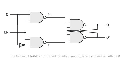
That alone is not memory yet, because $Q$ just follows $D$ all the time. So add an enable, EN, ANDed into both control paths. Figure 1 shows the four-NAND version.
| EN | D | $Q_{next}$ | |
|---|---|---|---|
| 0 | 0 | previous | hold |
| 0 | 1 | previous | hold |
| 1 | 0 | 0 | follows D |
| 1 | 1 | 1 | follows D |
With EN high the latch is transparent: $Q$ follows $D$ after a gate delay or two. With EN low it is opaque: $Q$ holds whatever $D$ was when EN fell. The characteristic equation is
$$Q_{next} = D \cdot EN + Q \cdot \overline{EN}$$
Figure 2 shows both phases.
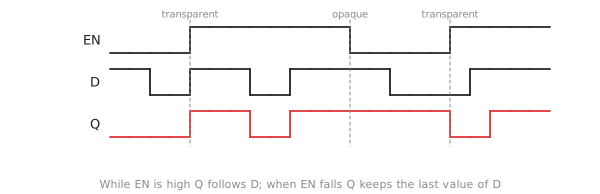
Notice that during the transparent phase every change on $D$ goes straight to $Q$, glitches included. If the logic feeding $D$ has a hazard, the latch reproduces it.
The transmission-gate version
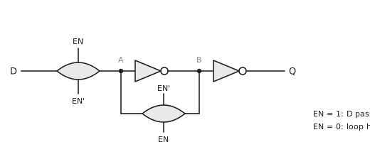
In silicon the D latch is usually built from transmission gates rather than NANDs (Figure 3). One transmission gate passes $D$ into the loop when EN is high; two inverters form the loop; a second transmission gate, open when EN is low, closes the feedback path so that the loop holds. Six transistors plus the enable inverter, the most compact form there is, and this is what a standard cell library uses.
The problem with levels
The D latch is level-sensitive: it is transparent for as long as EN is high, not just at an instant. In a synchronous system that causes trouble. Suppose $Q$ feeds combinational logic whose output comes back to $D$. While EN is high, a change on $D$ reaches $Q$, goes round through the logic, changes $D$ again, reaches $Q$ again, and so on. The latch can run through several state changes in one enable phase, and the value it ends up holding depends on the exact delays through the logic. That is a race, and the behaviour is decided by timing rather than by logic.
This is why synchronous design uses edge-triggered flip-flops, which capture $D$ at an instant rather than over an interval. Latches are still used deliberately in some high-performance designs, in a technique called time borrowing where alternating latches let a slow pipeline stage take time from its neighbours, but that is an advanced method with its own discipline, and everything in this course uses flip-flops.
Setup and hold
Even without a clock edge, the latch has timing requirements around the falling edge of EN, because that is the moment it captures. $D$ must be stable for a setup time $t_{su}$ before EN falls, or the latch may close on a half-changed value and end up in the unstable middle state. And $D$ must stay stable for a hold time $t_h$ after EN falls, while the feedback loop takes over from the input. Together these define a window around the capture point in which $D$ must not change. The same window, around the clock edge, governs every flip-flop, and section 3.1.6 treats it properly.
Practice Exercise
Problem 1. A D latch has $t_{su} = 2$ ns, $t_h = 1$ ns and a propagation delay of 3 ns. EN falls at 10 ns. When must $D$ stop changing, when may it change again, and when does the captured value appear at $Q$?
Solution
$D$ must be stable from 8 ns (setup) until 11 ns (hold). After 11 ns it can change freely; the latch is opaque. The captured value is at $Q$ by about 13 ns.
Problem 2. Why does putting two D latches in series with the same EN not fix the transparency race?
Solution
With the same enable, both are transparent at the same time and data passes through both as if neither were there. The fix is to give them opposite enables, so that one is opaque while the other is transparent. That is the master-slave arrangement, and it is the D flip-flop of the next article.
Problem 3. A D latch holds $Q = 1$ with EN low. $D$ glitches low for 1 ns. Does $Q$ change?
Solution
No. With EN low the latch is opaque. The glitch would only reach $Q$ if EN were high at the time, which is one reason to keep the transparent phase short and to make sure $D$ has settled before EN rises.
In the next article we put two D latches back to back with opposite enables and get the D flip-flop, which captures data at a clock edge instead of over a level.