Setup, Hold and Clock-to-Q
This is the last article of section 3.1, and it is about numbers. A design that works at 25 °C and 1.0 V can fail at 85 °C and 0.95 V, and the difference is often under 50 ps. Every digital design team spends a great deal of its time making sure the timing constraints in this article are met at every combination of process, voltage and temperature the product will see. The four parameters below are the foundation of that.
The four parameters
Setup time, $t_{su}$. The minimum time the D input must be stable before the clock edge. The master latch needs time to respond to D and develop a clear voltage difference on its internal nodes before the edge closes it. If D changes inside this time, the latch closes on a half-formed value, and the flip-flop can go metastable: its output sits between 0 and 1 and resolves at an unpredictable time, possibly a very long one. Typical values are 20 to 100 ps in a modern process, and a few hundred picoseconds in an older 180 nm one.
Hold time, $t_h$. The minimum time D must stay stable after the clock edge. Even once the edge has closed the master latch, the captured value takes a moment to establish itself, and a change on D immediately after the edge can chase it through. Typical values are 0 to 50 ps; some cells have a negative hold time, meaning D may change slightly before the edge.
Hold violations are the nastier of the two. A setup violation means the path is too slow, and slowing the clock or shortening the logic fixes it. A hold violation means the path is too fast: the new data arrives at the next flip-flop before that flip-flop has finished capturing the old data. Slowing the clock does nothing, since it does not change how early the data arrives after the edge. The only fix is to add delay in the data path.
Clock-to-Q delay, $t_{cq}$. The time from the clock edge to Q being valid at its new value. It has a maximum, used in setup analysis, and a minimum, used in hold analysis. Typically 50 to 150 ps.
Contamination delay, $t_{ccq}$. The earliest time after the edge at which Q may start to change. It is the lower bound on $t_{cq}$ and is what matters for hold: the next flip-flop must not see its D input move until its hold time has passed.
Figure 1 shows them on one diagram.
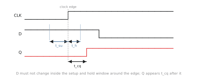
The window from $t_{su}$ before the edge to $t_h$ after it is the danger zone. Any transition of D inside it risks metastability.
The two constraints
Take the standard case: two flip-flops on the same clock with combinational logic between them (Figure 2).
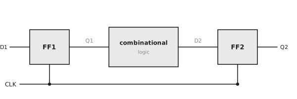
Setup. After a clock edge, Q1 is valid at $t_{cq,max}$, the logic takes up to $t_{pd,max}$, and D2 must be valid $t_{su}$ before the next edge:
$$t_{cq,max} + t_{pd,max} + t_{su} \leq T_{clk}$$
The setup slack is the difference between the right and left sides, and the design works if it is not negative. Setting it to zero gives the maximum clock frequency:
$$f_{max} = \frac{1}{t_{cq,max} + t_{pd,max} + t_{su}}$$
Hold. After the same edge, Q1 may start changing at $t_{ccq,min}$, the logic may pass that in as little as $t_{pd,min}$, and D2 must not change until $t_h$ after the edge:
$$t_{ccq,min} + t_{pd,min} \geq t_h$$
The hold slack is the left side minus the right. Notice that the clock period does not appear. Hold is about the same edge, not the next one, and that is why frequency cannot fix it.
At 3 GHz the period is 333 ps. Take 50 ps for setup, 80 ps for clock-to-Q, and 20 ps and 15 ps for skew and jitter (below), and about 170 ps is left for all the logic between two flip-flops, roughly ten to fifteen gates. That is why processor teams work so hard on their critical paths.
Skew and jitter
Two more things eat into the budget. Clock skew, $t_{skew}$, is the difference in arrival time of the clock at two flip-flops, from differing wire lengths and buffer loads in the clock tree. If FF2’s clock arrives later than FF1’s, the path has less than a full period. Clock jitter, $t_{jitter}$, is the cycle-to-cycle variation in the period from noise in the PLL and the supply. The full setup constraint is
$$t_{cq,max} + t_{pd,max} + t_{su} + t_{skew} + t_{jitter} \leq T_{clk}$$
Skew can also help or hurt hold, depending on its sign, and section 3.2 goes into the clock network properly.
PVT corners
Chips are not all identical. Doping, oxide thickness and lithography vary from wafer to wafer and across a wafer, so transistors are faster or slower than nominal. The supply voltage droops under load. The temperature depends on the workload. The three are the process, voltage and temperature corners.
Process corners are named by the NMOS and PMOS speed: SS is slow-slow, FF is fast-fast, TT is typical, and FS and SF have the two device types mismatched. Lower voltage and higher temperature slow transistors down (at very advanced nodes low temperature can slow some devices too, but hot and slow is the usual worst case).
| Constraint | Worst corner |
|---|---|
| setup | slow process, low voltage, high temperature |
| hold | fast process, high voltage, low temperature |
Setup fails on slow paths, so it is checked where everything is slowest. Hold fails on fast paths, so it is checked where everything is fastest. A design that meets setup at the slow corner and fails hold at the fast one is a failed design; both have to pass. Sign-off tools run all of these, and also on-chip variation, where different flip-flops on the same die are at different points at the same time.
Practice Exercise
Problem 1. $t_{cq,max} = 80$ ps, $t_{ccq,min} = 25$ ps, $t_{su} = 45$ ps, $t_{h} = 20$ ps, and the logic has $t_{pd,max} = 200$ ps and $t_{pd,min} = 40$ ps. What is the minimum clock period, is hold met, and what is the maximum frequency?
Solution
Minimum period: $80 + 200 + 45 = 325$ ps. Hold slack: $25 + 40 - 20 = 45$ ps, so hold is met. Maximum frequency: about 3.08 GHz.
Problem 2. The same design at the slow corner has every delay 40 percent larger. Does it still meet setup at 325 ps?
Solution
$t_{cq} = 112$ ps, $t_{pd} = 280$ ps, $t_{su} = 63$ ps, total 455 ps. At a 325 ps period the setup slack is −130 ps. The design fails at the slow corner. It has to be re-targeted to about 2.2 GHz, or the critical path shortened.
Problem 3. Two flip-flops are connected by almost no logic, $t_{pd,min} = 5$ ps. $t_{ccq,min} = 30$ ps and $t_h = 40$ ps. Is hold met, and if not, what is the fix?
Solution
Hold slack is $30 + 5 - 40 = -5$ ps, a violation. Add delay in the data path: at least 5 ps, in practice a buffer of 20 to 40 ps for margin. Running the clock slower would not help at all.
Section 3.1 in one table
| Element | Inputs | Triggered by | Property |
|---|---|---|---|
| cross-coupled inverters | none | nothing | bistable but uncontrolled |
| SR latch | S, R | level | has a forbidden state |
| D latch | D, EN | level | transparent while enabled |
| D flip-flop | D, CLK | edge | the synchronous storage element |
| JK flip-flop | J, K, CLK | edge | can toggle |
| T flip-flop | T, CLK | edge | toggle only, for counters |
| Parameter | Symbol | Governs | Typical, 7 nm |
|---|---|---|---|
| setup time | $t_{su}$ | setup | 20 to 100 ps |
| hold time | $t_h$ | hold | 0 to 50 ps |
| clock-to-Q, max | $t_{cq,max}$ | setup | 50 to 150 ps |
| contamination delay | $t_{ccq,min}$ | hold | 20 to 60 ps |
Section 3.2 takes the flip-flop and the clock and builds the discipline of synchronous design around them, starting with the choice between synchronous and asynchronous design and why the industry made it.