How Silicon Remembers
This is the first article of Module 3, and it starts with a problem that everything in Modules 1 and 2 cannot solve: remembering something. A combinational circuit has no past. Its outputs are a function of its present inputs and nothing else. This article is about why that is, and about the one idea, feedback, that gets round it.
The toggle switch
Take a simple job: a light that toggles. Press the button, the light comes on; press again, off; again, on. Now try to write that as a Boolean function. The output depends on how many times the button has been pressed, modulo 2, and the circuit only ever sees whether the button is pressed now. The information it needs is not in its inputs. The toggle cannot be built from combinational logic, and neither can anything else that depends on history.
Formally, a combinational circuit is a function $f: {0,1}^n \to {0,1}^m$: one output for each input pattern, always the same. That is a useful property for verification, since you can check all $2^n$ inputs and be done. It is exactly the wrong property for the toggle, which has to produce different outputs for identical inputs depending on what happened in between. The circuit needs to keep something from one event to the next. It needs memory.
Feedback
The idea is to connect a circuit’s output back to one of its inputs. Then the output at any moment depends on the external inputs and on what the output was a moment ago, which is a piece of history. All digital memory works this way. The job is to control the feedback so that it gives stable, useful behaviour rather than oscillation.
Try the simplest case first: one inverter with its output wired to its input (Figure 1).
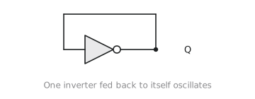
If the output is 0, the input is 0, so the output becomes 1, so the input is 1, so the output becomes 0, and so on. It oscillates with a period set by the inverter’s delay. That is how a ring oscillator works and it is useful for generating a clock, but it cannot store a bit. One inverter has one equilibrium point, at the middle of its transfer curve, and that point is unstable. What we need is a circuit with two stable states, so that it rests in one until it is deliberately pushed to the other.
Two inverters back to back
Now connect two inverters in a loop, the output of each to the input of the other (Figure 2).

Call the nodes A and B. If A is 0, the first inverter drives B to 1, and the second inverter drives A to 0. Consistent; the circuit stays there. If A is 1, B is driven to 0 and A is driven to 1. Also consistent. Two stable states, and the circuit stays in either one indefinitely, drawing only leakage current.
There is a third equilibrium, both nodes at half the supply voltage, but it is unstable: the slightest noise tips the circuit into one of the stable states. We will meet this middle point again as metastability.
A circuit with two stable states can store one bit. Assign A = 0 to a stored 0 and A = 1 to a stored 1, and you have the most primitive digital memory there is. Every memory element in this module, and every register file and cache in any processor, comes down to this loop.
The SRAM cell
The cross-coupled pair is the core of the static RAM cell. A complete cell adds two access transistors, as in Figure 3.
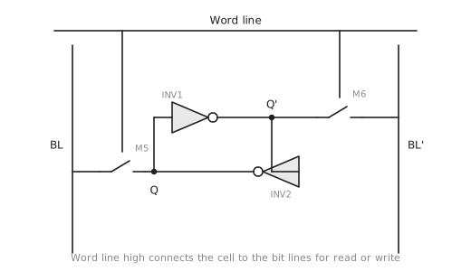
When the word line is high, the access transistors connect the two internal nodes to the bit lines so that the cell can be read or written. When it is low, the cell is isolated and holds its value. Two inverters at two transistors each plus two access transistors make the 6T cell. In a 5 nm process a cell is roughly 0.02 µm², and a 16 MB cache holds about 134 million of them, some 800 million transistors before counting decoders, sense amplifiers and the rest.
Where this section goes
The inverter pair holds a bit but gives no controlled way to write it. The rest of section 3.1 adds that:
- The SR latch: set and reset inputs on the cross-coupled pair.
- The D latch: no forbidden state, and an enable.
- The D flip-flop: edge-triggered, the element every synchronous design is built from.
- JK and T flip-flops: toggle behaviour for counters.
- Timing parameters: setup, hold and clock-to-Q, the numbers that decide whether a design works.
Practice Exercise
Problem 1. A combinational circuit computes the majority of A, B and C. Can it remember whether A was ever 1?
Solution
No. Its output depends on the present A, B and C only. Once A returns to 0, with B and C at 0, the output is 0 and nothing in the circuit records that A was ever anything else. Remembering that would need a sequential element that latches when A first goes high.
Problem 2. Both nodes of a cross-coupled inverter pair are forced to 0 by external drivers, and the drivers are then released. What happens?
Solution
With A = B = 0 both inverters want to drive their outputs high. Whichever node rises first wins: if A gets above the switching threshold first it drives B low, which reinforces A high. For a moment the circuit is near the unstable midpoint, and which way it falls depends on noise and mismatch between the two inverters. The outcome cannot be predicted. This is exactly what happens on leaving the forbidden state of an SR latch.
Problem 3. How many cells and how many transistors are in the storage array of a 32 KB SRAM?
Solution
32 KB is $32 \times 1024 \times 8 = 262{,}144$ bits, so 262,144 cells, and at six transistors each about 1.57 million transistors. The decoders, sense amplifiers and write drivers add perhaps another 30 to 50 percent.
In the next article we replace the two inverters with two NAND gates and get the SR latch, the first memory element with proper set and reset inputs.