Shift Registers
The register of the last article holds data. A shift register moves it. How does a single serial wire turn into an 8-bit byte the rest of the circuit can use at once? That is what the shift register does, and this article covers its four forms.
The chain
Take $N$ D flip-flops and connect the Q of each to the D of the next. The first D is the serial input and the last Q is the serial output (Figure 1). At every rising edge each flip-flop takes the value its neighbour had, so data moves one place along the chain per clock, and a bit entered at one end comes out of the other $N$ cycles later.
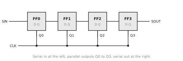
The four forms differ only in how data goes in and comes out: one bit at a time, serially, or all bits at once, in parallel.
Serial in, serial out
Nothing but the chain. A bit goes in, and $N$ clocks later it comes out: a delay line of exactly $N$ cycles, holding the last $N$ bits of the stream (Figure 2).
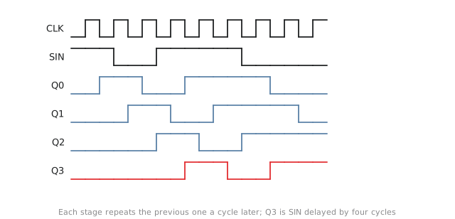
Used for pipeline alignment, for the taps of a digital filter, and anywhere a signal needs a fixed number of cycles of delay.
Serial in, parallel out
The chain with every Q brought out. Shift in $N$ bits and the whole word is on the parallel outputs. Receiving the byte 10110100, most significant bit first, the first bit shifts through to the far end over eight clocks and the outputs read 10110100 = 0xB4. This is serial-to-parallel conversion, and it is the receive half of SPI, UART and I²C. The parallel outputs are only meaningful after all $N$ bits are in, so a frame-complete or data-valid signal accompanies them.
Parallel in, serial out
The reverse. Each flip-flop’s D input has a 2-to-1 mux choosing between the parallel input, when LOAD is high, and the neighbour’s Q, when it is low (Figure 3). Assert LOAD for one cycle to take the word, then shift for $N$ cycles to send it out one bit at a time from the last Q. This is the transmit half of the same interfaces.
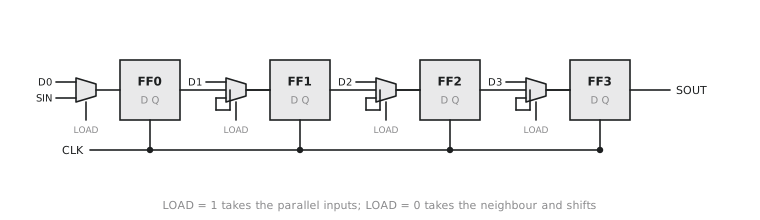
The mux at each stage,
$$D_{actual}[i] = LOAD ;?; D[i] : Q[i-1]$$
with the serial input in place of $Q[-1]$ at the first stage, is the pattern behind every shift register with more than one mode. The universal shift register in article 3.4.4 has a 4-to-1 version.
Parallel in, parallel out
That is just the register of the last article. There is no shifting.
| Form | In | Out | Use |
|---|---|---|---|
| SISO | serial | serial | delay line |
| SIPO | serial | parallel | serial-to-parallel: SPI and UART receive |
| PISO | parallel | serial | parallel-to-serial: SPI and UART transmit |
| PIPO | parallel | parallel | an ordinary register |
Every microcontroller’s SPI peripheral contains exactly a PISO on the MOSI side and a SIPO on the MISO side, usually called the transmit and receive buffers.
Direction
The chains above shift one way. A bidirectional register adds a direction control and a second serial input so that data can move towards either end; the universal shift register does this.
Practical points
Bit order matters: protocols specify whether the first bit on the wire is the most or least significant, and which end of the register is the input decides which you get. When the serial clock is not the system clock, as it is not for an SPI slave, the parallel word has to be brought into the system clock domain through a synchroniser on the data-valid signal, as in section 3.2.
Practice Exercise
Problem 1. An 8-bit SIPO receives, most significant bit first, 0, 1, 1, 0, 1, 0, 0, 1. What is the parallel output?
Solution
01101001, which is 0x69.
Problem 2. A PISO holds 0xA5. After a load and five shifts (with 0 shifted in), what remains, and what came out?
Solution
Starting from 10100101 and shifting out the top bit each time: 1, 0, 1, 0, 1 come out, and 00000101 = 0x05 remains.
Problem 3. Draw a 4-bit SIPO and count its external connections.
Solution
Four flip-flops in a chain, SIN into the first, each Q to the next D and to a parallel output. Inputs: SIN, CLK and a reset, three. Outputs: Q0 to Q3, four. Seven wires; a serial output is just Q3 again.
The next article looks at what shift registers get used for beyond serial conversion: delay lines, UART framing, ring counters, pseudo-random sequences and scan chains.