The D Flip-Flop
In the last article the D latch had a problem: it is transparent for as long as its enable is high, and data can race round a feedback loop several times in one enable phase. What synchronous design needs is an element that captures its input at an instant, not over an interval. That instant is the clock edge, and the element is the D flip-flop. I would say it is the most important circuit in digital design. Every register, every pipeline stage, every state variable of every state machine, every FIFO pointer is one of these.
Master and slave
Put two D latches in series and give them opposite enables (Figure 1). The first, the master, is enabled while the clock is low. The second, the slave, is enabled while the clock is high.
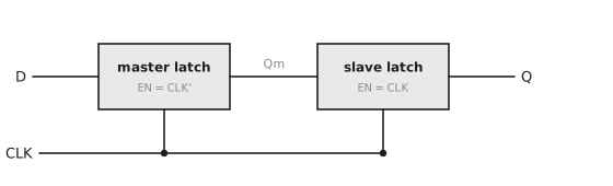
While the clock is low the master is transparent and follows $D$; the slave is opaque and holds $Q$ steady. When the clock rises, the master closes and keeps whatever $D$ was just before the edge, and at the same moment the slave opens and passes that value to $Q$. Now $Q$ has changed, but $D$ is cut off from $Q$ because the master is closed. Anything that comes back round to $D$ cannot get through until the next rising edge. The race is broken.
The net behaviour: $Q$ takes the value of $D$ at the rising edge of the clock, and holds it until the next rising edge. Nothing $D$ does in between matters (Figure 2).
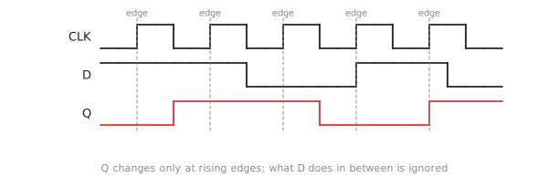
The delay from the clock edge to $Q$ settling is the clock-to-Q delay, $t_{cq}$, typically 50 to 100 ps in a 7 nm cell.
Why edges matter
Edge triggering changes the whole design method. The output changes for an instant and then holds for a full period, so the logic it drives has the whole period to settle. The input only has to be stable in a small window around the edge, and can do what it likes the rest of the time. Every flip-flop on a clock updates at the same edge, so the whole state of the design changes at once, which is what makes a large design analysable. And the problem splits cleanly: the combinational logic decides what the next state is, and the flip-flops decide when it takes effect.
In silicon
The transmission-gate latch from the last article, doubled, gives a 12-transistor flip-flop plus the clock inverter: two transmission gates and two inverter pairs. The master’s gate passes on clock low and the slave’s on clock high, using the clock and its complement. A flip-flop cell is well under a square micron in a modern process.
A flip-flop that captures on the falling edge is the same circuit with the enables swapped. Its symbol has a bubble on the clock input. Unless I say otherwise, “flip-flop” in this course means rising-edge.
Synchronous reset
Most flip-flops have a reset that forces $Q$ to 0, and there are two kinds.
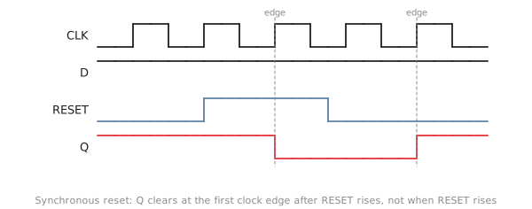
A synchronous reset is just logic on the D input: $D_{actual} = D \cdot \overline{RESET}$. Asserting RESET does nothing until the next clock edge, at which point the flip-flop captures 0 (Figure 3). The flip-flop stays fully synchronous, a glitch on RESET between edges cannot reach $Q$, and a reset pulse shorter than a clock period may be missed if it falls between edges.
Asynchronous reset
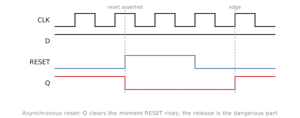
An asynchronous reset bypasses the clock. It is wired into the latch loops directly, and $Q$ goes to 0 the moment RESET is asserted (Figure 4).
You need this at power-up, when there is no clock yet and the flip-flops have to be put into a known state, and in safety logic where a fault must stop things now rather than at the next edge.
The danger is in releasing it. Assertion can happen any time. But when RESET is released, the flip-flop goes back to normal operation, and if the release happens within the setup-hold window of a clock edge the flip-flop can go metastable. With thousands of flip-flops released at once, some may come out of reset a cycle before others, and the design starts in an inconsistent state. So the usual practice is asynchronous assertion, synchronous release: the reset is asserted immediately but its release is passed through a pair of flip-flops on the clock so that it lines up with an edge. Section 3.2 comes back to this.
The enable input
An enable lets the flip-flop hold its value on some cycles:
$$D_{actual} = EN ;?; D : Q$$
With EN low the flip-flop reloads its own output, so it holds. This is a 2-to-1 mux on the D input, and it is how a processor register that is only written on some cycles, or a pipeline stage that stalls, is built. It is not done by gating the clock. Clock gating is a separate power-management technique done at the clock-tree level with special cells, as Module 2 discussed, and never as a way of implementing a per-register enable.
Practice Exercise
Problem 1. A flip-flop has $t_{su} = 2$ ns, $t_h = 0.5$ ns and $t_{cq} = 3$ ns. The clock rises at 0 and $D$ changed at −3 ns. Is setup met? When is the new $Q$ valid?
Solution
$D$ had to be stable by −2 ns and was stable from −3 ns, so setup is met with 1 ns to spare. It does not change again, so hold is met. $Q$ is valid at 3 ns.
Problem 2. Why is gating the clock a bad way to implement a per-register enable?
Solution
If the enable changes while the clock is high, the gate produces a partial pulse, a spurious edge that clocks the register at the wrong moment. The gating logic also adds skew to the clock, since the gated flip-flops see a later edge than the rest. Use a mux on D for enables, and leave clock gating to the dedicated latch-based cells that the power tools insert.
Problem 3. An active-low asynchronous reset is released 0.8 ns before a clock edge, and the flip-flop’s setup time is 1 ns. Is there a problem?
Solution
Yes. The release falls inside the window before the edge, and the flip-flop may go metastable. In a large design some flip-flops would leave reset on that edge and others a cycle later. The fix is to synchronise the release: pass the reset through two flip-flops on the system clock before it reaches the design.
The D flip-flop is the workhorse, but two variants, the JK and T flip-flops, express the toggle operation directly and turn up in older designs and in counter theory. They are the subject of the next article.