The Universal Shift Register
The last two articles treated the shift register forms as separate circuits. In a processor or a DSP you want one register that can do any of them under program control: load an immediate value, shift either way, hold between operations. The universal shift register does all four, selected by two mode bits, and it has existed as a single chip, the 74194, since the TTL era.
The mode table
| S1 | S0 | Operation |
|---|---|---|
| 0 | 0 | hold |
| 0 | 1 | shift right: $Q[i] \leftarrow Q[i+1]$, SR_IN enters at the top |
| 1 | 0 | shift left: $Q[i] \leftarrow Q[i-1]$, SL_IN enters at the bottom |
| 1 | 1 | parallel load: $Q[i] \leftarrow D[i]$ |
With $Q[N-1]$ as the most significant bit, shifting right moves data towards bit 0.
The circuit
For each bit, compute all four candidate next values and pick one with a 4-to-1 mux:
$$D_{actual}[i] = \begin{cases} Q[i] & S = 00 \ Q[i+1] & S = 01 \ Q[i-1] & S = 10 \ D[i] & S = 11 \end{cases}$$
At the top bit the shift-right input is the external SR_IN, and at the bottom bit the shift-left input is SL_IN. One mux and one flip-flop per bit, with the mode bits shared (Figure 1).
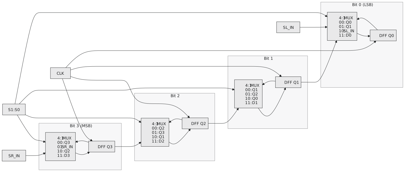
Figure 2 runs through all four modes: load 1010, hold, shift right twice with 1 then 0 entering, shift left twice with 0 then 1 entering, load 0110, hold.
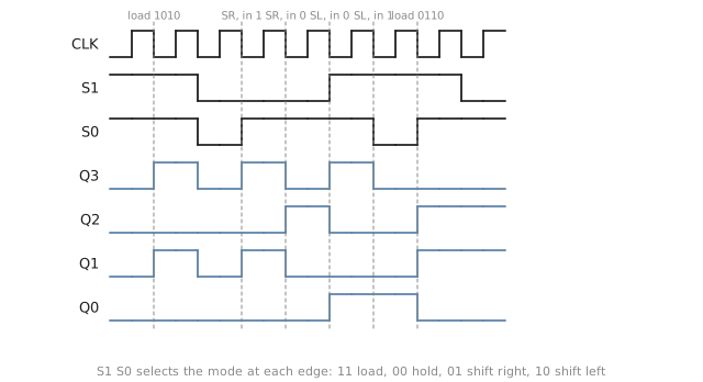
Every transition is clean, because every flip-flop is on the same clock and the mode is sampled at the edge.
The 74HC194
The 74HC194 is this circuit in a 16-pin package: clock, an asynchronous clear, S0 and S1, serial inputs DSR and DSL, four parallel inputs and four outputs. Its function table is the mode table above plus a row for the clear, which overrides everything and zeroes the outputs immediately. That clear is the one asynchronous thing on the chip; the four modes are synchronous.
Cascading
Two of them make an 8-bit register. For shifting right, the bottom output of the high chip feeds the DSR input of the low chip; for shifting left, the top output of the low chip feeds the DSL input of the high chip. Both chips share the clock, clear and mode bits and load their own four parallel inputs at once. Any width follows the same pattern.
The 4-to-1 mux in front of each flip-flop is the general pattern of datapath design: compute every possible next value, then select one with the operation code. An ALU is the same thing with add, AND, OR and XOR results in place of the four shift modes.
Size and speed
A 4-bit register is four flip-flops and four 4-to-1 muxes, perhaps sixteen gate equivalents of mux. The critical path is a mux plus a flip-flop’s setup, the same for every bit, with no ripple, so it runs at several hundred megahertz in any modern process and is never the bottleneck.
Practice Exercise
Problem 1. From $Q = 1011$ with SR_IN = 0 and SL_IN = 1, trace two right shifts, and separately two left shifts.
Solution
Right: 0101, then 0010, with 0 entering at the top each time. Left, from 1011: 0111, then 1111, with 1 entering at the bottom each time.
Problem 2. Make the register do an arithmetic right shift.
Solution
Connect SR_IN to $Q[3]$. Each right shift then copies the sign bit into the vacated top position. From 1011 (−5) one shift gives 1101 (−3), which is −5 divided by 2 rounded towards negative infinity. That is how a processor’s ASR instruction is built.
Problem 3. How many 74HC194s for a 16-bit register, and how are they connected for right shifts?
Solution
Four. For right shifts the $Q[0]$ of each chip feeds the DSR of the next chip down, the external serial input feeds the DSR of the top chip, and $Q[0]$ of the bottom chip is the serial output. All four share clock, clear and mode.
That completes registers. Section 3.5 is about counters, starting with the ripple counter built from the T flip-flops of section 3.1 and why it is slower than it looks.