Designing with Building Blocks
This is the last article of Module 1. We have the blocks now: multiplexers, decoders, encoders, comparators. In this article I want to talk about how they get used, because there is a shift in the way you look at a circuit that happens at about this point, and it is worth making explicit.
Seeing blocks instead of gates
A beginner looks at a schematic and sees gates: AND, OR, XOR, a field of symbols. An experienced designer looks at the same schematic and sees a comparator feeding a mux, a decoder driving some enables, an adder. The difference is not cosmetic. It is the difference between someone who can design a flip-flop and someone who can design a processor.
When you write a sentence you are not thinking about letters. Once a block is understood and characterised, its function, its timing, its size, you should stop thinking about what is inside it. A mux is not “two ANDs, an OR and an inverter”. A mux is “output = select ? B : A”. Full stop, move up a level.
This is also why hardware description languages exist. Verilog’s module lets you describe a circuit as blocks connected by their interfaces, and instantiate a block without caring about its contents. The tools translate to gates. Learning Verilog is learning to write down this kind of hierarchical thinking.
A design exercise: a small ALU
Let us decompose a real specification the way it is done in practice. We will not implement everything, since the adder is Module 2’s job, but we will get to the block diagram.
Specification. A 4-bit ALU with eight operations selected by a 3-bit opcode:
| Opcode | Operation | Description |
|---|---|---|
| 000 | A + B | unsigned add |
| 001 | A − B | unsigned subtract |
| 010 | A | pass A through |
| 011 | A AND B | bitwise |
| 100 | A OR B | bitwise |
| 101 | A XOR B | bitwise |
| 110 | A = B | 0001 if equal, else 0000 |
| 111 | A > B | 0001 if greater, else 0000 |
Step 1: identify the blocks. Add and subtract need an adder/subtractor; subtraction is $A + B’ + 1$ in two’s complement, so one adder with an invert-B control does both. Pass A is wires. AND, OR and XOR are four gates each. Equality and magnitude are the comparators from the last article.
Step 2: draw the block diagram. Every block computes its result at the same time, all the time, and an 8-to-1 mux at the output picks the one the opcode asks for (Figure 1).
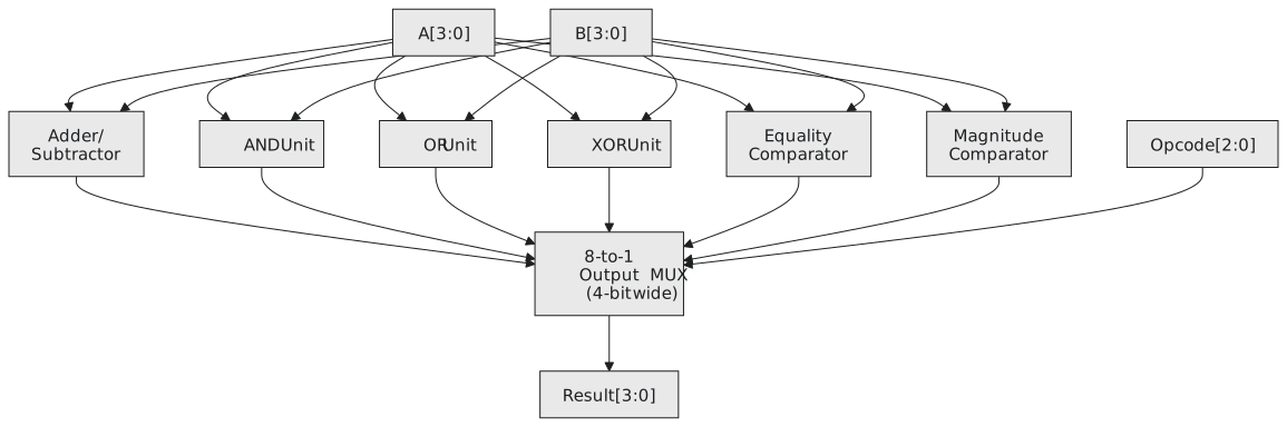
Step 3: identify the control. The opcode drives the mux select directly; no decoder is needed. The adder’s subtract input is simply “opcode equals 001”.
Step 4: notice what is missing. The adder/subtractor. We know its interface, two 4-bit inputs, a subtract control, a 4-bit result and a carry out, but not its inside. That is deliberate, and it is how real design works. You define the interfaces first, then implement the blocks, and several people can implement different blocks at the same time. The block diagram is the document an architect hands to a team: “you build the adder to this interface, you build the comparator to that one.” That decomposition is often the most valuable work on a project.
Hierarchy
The same approach applies at every scale:
| Level | What you see | Built from |
|---|---|---|
| Transistor | NMOS and PMOS switches | silicon |
| Standard cell | NAND, NOR, flip-flop | a few transistors |
| Functional unit | adder, mux, comparator | cells |
| Subsystem | ALU, register file, cache | functional units |
| Chip | CPU, GPU, SoC | subsystems |
| System | computer, phone | chips |
Each level hides what is below it. The CPU designer does not think about transistors and the system architect does not think about standard cells. Software calls this encapsulation, and Verilog’s module with its input and output ports is the hardware version.
Buses
When several units need to talk to each other, wiring every unit to every other needs $O(n^2)$ connections. Instead, systems use a bus: a shared set of wires with rules about who drives it when.
The hardware problem is that two units driving the bus at once fight each other, and the solution is the tri-state buffer from section 1.3, which can drive high, drive low, or disconnect. Only one buffer on the bus is enabled at a time, and a decoder chooses which (Figure 2).
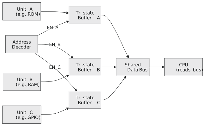
This is how memory-mapped I/O works on every microcontroller. When your C code reads from 0x40020000 on an STM32, which is a GPIO register, the address decoder enables the GPIO block’s driver and its register contents appear on the data bus.
One thing to know: inside modern FPGAs and ASICs, tri-state buses are mostly avoided, because they complicate timing analysis and FPGA fabrics do not support them internally. On-chip, the usual replacement is a mux: a wide mux selects among unit outputs in ordinary logic. Tri-state drivers survive at the pins, for external buses.
Module 1 in one page
Numbers (section 1.1) are the language. Every address, opcode and data value is a binary number, and when you read a simulation waveform you read hex.
Boolean algebra (section 1.2) is how we reason about logic. Without it there is no way to prove two circuits equivalent or to simplify one.
Gates (section 1.3) connect the algebra to silicon. NAND and NOR are universal and they are the cheap CMOS gates, which is why real netlists are made of them.
Karnaugh maps (section 1.4) are the design process in miniature: truth table in, minimal expression out. Synthesis tools do the same thing at scale.
Building blocks (section 1.5) lift the level of abstraction so that you can read a block diagram without reverse-engineering the gates.
Self-check
Be honest with yourself here. If any of these is shaky, go back to the section before continuing.
Numbers: convert between decimal, binary and hex without a calculator; add and subtract in binary and detect overflow; negate a two’s complement number.
Boolean algebra: apply De Morgan to any expression and check it with a truth table; simplify a 4-variable expression by hand; state the duality principle.
Gates: write the seven truth tables from memory; build any 2-variable function from NAND gates only; explain why NAND is universal.
Karnaugh maps: fill in a 4-variable map from a minterm list; find the prime implicants and the essential ones; write the minimal SOP; use don’t-cares.
Blocks: write the 2-to-1 mux equation and draw it; implement a 3-variable function with a 4-to-1 mux; explain why a decoder produces minterms; derive the 4-to-2 priority encoder; build a 4-bit equality comparator and explain MSB-first magnitude comparison; explain signed versus unsigned comparison.
Design: decompose a small specification into blocks; explain what a tri-state buffer is for; explain how hierarchy maps onto Verilog modules.
Practice Exercise
Problem 1. A 4-bit ALU supports ADD, AND, OR and PASS_A, with a 4-to-1 mux on the output. What connects to each mux input, and what drives the select?
Solution
$I_0$ is the adder output, $I_1$ is A AND B, $I_2$ is A OR B, $I_3$ is A itself. A 2-bit opcode drives $S_1 S_0$. Since every input is four bits wide, this is really four 4-to-1 muxes sharing one pair of select lines, or one 4-bit-wide mux.
Problem 2. Three devices drive a 4-bit bus. What happens if you leave out the tri-state buffers and connect their outputs directly?
Solution
All three drive the bus at all times. When two drive different levels, one output’s pull-up transistor and the other’s pull-down are connected through the wire: a low-resistance path from supply to ground. Current flows continuously, the wire settles at an undefined voltage, and the drivers can be damaged. In simulation you would see X on the bus. In hardware you see a hot chip and a broken system.
Problem 3. An engineer says a 4-input LUT is a 16-to-1 mux. Explain.
Solution
A 4-input LUT stores one output bit for each of the 16 input combinations, so it has 16 configuration bits. Those are the 16 data inputs of the mux; the four logic inputs are the select lines. For inputs 0101, say, the mux passes data input 5, which holds the truth table entry for that row. Any 4-variable function can be loaded into the 16 bits, so one LUT implements any of them.
Module 2 starts with the half adder, two gates and two outputs, and builds up through the full adder and the ripple-carry adder to the carry-lookahead adder, which is the same most-significant-bit-first thinking we used in the comparator applied to addition. By the end of it the box labelled “adder/subtractor” in Figure 1 will be a circuit you have designed yourself.