Multi-Input Gates, Compound Cells, Tri-State and Transmission Gates
In the last article we went through the seven basic gates. If you open a real standard cell library you will find a lot more than seven cells: AND2, AND3, AND4, AOI21, AOI22, OAI21, TBUF, and hundreds of others. In this article I want to go through the important additions and explain why each one exists. The common thread is that a compound cell does two levels of logic in one transistor stage, which saves both transistors and delay. Knowing these cells exist is what lets you read a synthesized netlist and a timing report without being surprised.
Multi-input AND, OR and XOR
AND and OR are associative:
$$A \cdot B \cdot C = (A \cdot B) \cdot C = A \cdot (B \cdot C)$$
$$A + B + C = (A + B) + C = A + (B + C)$$
So a 4-input AND is well defined without any bracketing: the output is 1 only when all four inputs are 1. Its truth table has 16 rows and exactly one 1, in the last row. A 4-input OR has one 0, in the first row. Libraries offer AND2, AND3 and AND4, and the same for OR, NAND and NOR. You rarely pick these by hand; the synthesis tool chooses the width.
XOR is also associative, and the multi-input version has a useful meaning: an N-input XOR outputs 1 when an odd number of its inputs are 1. This is the parity function. Here is the 3-input case worked out:
| A | B | C | A⊕B | (A⊕B)⊕C | Number of 1s | Odd? |
|---|---|---|---|---|---|---|
| 0 | 0 | 0 | 0 | 0 | 0 | no |
| 0 | 0 | 1 | 0 | 1 | 1 | yes |
| 0 | 1 | 0 | 1 | 1 | 1 | yes |
| 0 | 1 | 1 | 1 | 0 | 2 | no |
| 1 | 0 | 0 | 1 | 1 | 1 | yes |
| 1 | 0 | 1 | 1 | 0 | 2 | no |
| 1 | 1 | 0 | 0 | 0 | 2 | no |
| 1 | 1 | 1 | 0 | 1 | 3 | yes |
Every row with output 1 has an odd count of 1s. This is why XOR trees are used for parity generation and checking (in DRAM error correction, serial protocols and RAID) and for CRC, which is polynomial division modulo 2.
Chain or tree
When you need a wide gate, there are two ways to build it from 2-input cells, and the choice matters for timing. Figure 1 shows both for a 4-input XOR.
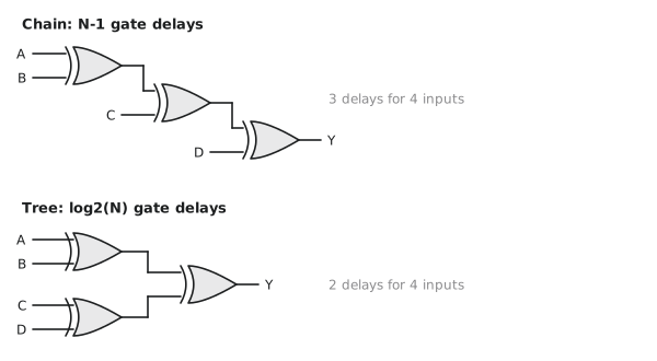
A chain of N inputs is N−1 gate delays deep. A tree is $\log_2 N$ deep. For a 16-input XOR that is 15 delays against 4. Synthesis tools build trees on their own when timing is tight, and the easiest way to let them is to write the reduction operator in Verilog and leave the structure to the tool:
assign parity = ^data_bus; // synthesis builds an XOR tree
AND-OR-INVERT and OR-AND-INVERT cells
This is where standard cell libraries get interesting. An AOI or OAI cell implements a two-level Boolean function in a single CMOS stage, with fewer transistors than the separate gates would need.
Take AOI21, which stands for AND-OR-INVERT with a 2-input AND and one extra OR input:
$$Y = \overline{(A \cdot B) + C}$$
Built from separate gates it would need an AND (6 transistors), an OR (6) and an inverter (2), 14 transistors over two gate delays. As a single CMOS cell it needs 6 transistors: in the pull-down network A and B are in series (the AND part) with C in parallel with them (the OR part), and the pull-up network is the complementary arrangement. The inversion comes for free because a single CMOS stage always inverts. Six transistors, one gate delay.
| A | B | C | A·B | (A·B)+C | AOI21 output |
|---|---|---|---|---|---|
| 0 | 0 | 0 | 0 | 0 | 1 |
| 0 | 0 | 1 | 0 | 1 | 0 |
| 0 | 1 | 0 | 0 | 0 | 1 |
| 0 | 1 | 1 | 0 | 1 | 0 |
| 1 | 0 | 0 | 0 | 0 | 1 |
| 1 | 0 | 1 | 0 | 1 | 0 |
| 1 | 1 | 0 | 1 | 1 | 0 |
| 1 | 1 | 1 | 1 | 1 | 0 |
The other common members of the family are AOI22, $Y = \overline{(A \cdot B) + (C \cdot D)}$, at 8 transistors against 16 or more for separate gates, and OAI21, $Y = \overline{(A + B) \cdot C}$, which is the dual of AOI21.
The general rule is that sum-of-products expressions map onto AOI cells and product-of-sums expressions map onto OAI cells. Two-level logic minimizers produce exactly these forms, so technology mapping onto AOI and OAI cells is very efficient. When you synthesize against a real library you will see these cells everywhere in the netlist, and you will sometimes see a timing report that shows one and a half gate delays where you expected three. That is the tool doing its job.
Tri-state buffers
Every gate so far has two output states, HIGH and LOW. A tri-state buffer adds a third, called high impedance or High-Z, in which the output is effectively disconnected from the wire. Figure 2 shows the symbol.
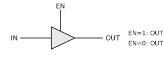
| EN | IN | OUT |
|---|---|---|
| 0 | 0 | Z |
| 0 | 1 | Z |
| 1 | 0 | 0 |
| 1 | 1 | 1 |
There are also active-low enable variants, where EN_N = 0 turns the output on.
The reason tri-state exists is the shared bus. If several devices need to drive the same wire, ordinary outputs cannot be connected together: two drivers pulling in opposite directions would fight, a condition called bus contention. Large current flows from one driver’s pull-up through the other’s pull-down, the wire sits at some voltage in the middle, and in a bad case something gets damaged. With tri-state drivers, only one device enables its output at a time and all the others float. Figure 3 shows the arrangement.
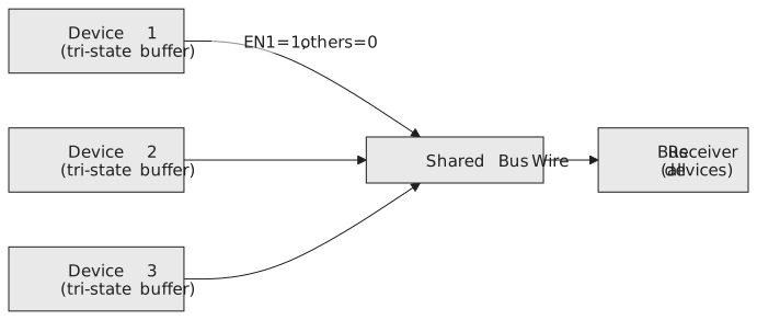
A bus arbiter makes sure exactly one enable is HIGH at any time. Getting that arbitration wrong is a real hazard on a PCB or in a custom chip, and even a brief overlap between two drivers is a short circuit. FPGA tools will mostly stop you from doing it inside the fabric, because modern FPGA routing does not support internal tri-state buses at all. Where you will still meet tri-state is at the I/O pads (bidirectional GPIO pins) and on off-chip buses such as DRAM data buses.
Open-drain outputs
A close relative is the open-drain output, called open-collector when the transistor is bipolar. An open-drain output can pull the wire LOW through its NMOS transistor, or release it to High-Z. It cannot drive HIGH. The HIGH level comes from an external pull-up resistor to VDD, as in Figure 4.
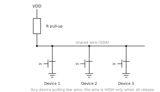
When several open-drain outputs share a wire, the wire is LOW if any device pulls it low, and HIGH only when all of them have released it. This is a wired-AND: the topology does the AND for free, without any gate.
The I²C bus, which connects sensors, EEPROMs and small peripherals in nearly every embedded system, is built entirely on this. Both SDA and SCL are open-drain. Any device can pull a line low, and the wired-AND is what makes clock stretching possible: a slow peripheral holds SCL low until it is ready, and nobody needs any extra arbitration hardware.
Transmission gates
The last cell type worth knowing is the transmission gate, or pass gate. It is one NMOS and one PMOS connected in parallel with complementary control signals, as in Figure 5.
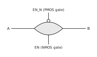
When EN is 1 (and EN_N is 0) both transistors conduct and A is connected to B through a low resistance. When EN is 0 both are off and the connection is broken.
Two properties make this useful. First, it is bidirectional; a signal passes from A to B or from B to A, unlike a normal gate output. Second, it passes both logic levels cleanly. An NMOS on its own passes a 0 well but loses a threshold voltage when passing a 1, and a PMOS has the opposite problem. In parallel they cover for each other.
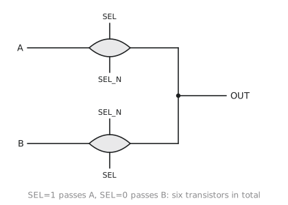
You meet transmission gates in three places. A 2:1 multiplexer built from two transmission gates and an inverter for the select signal uses six transistors, against about twelve for an AND-OR implementation, which is why library MUX cells are often built this way (Figure 6). The 6-transistor SRAM cell uses two pass transistors to connect the storage node to the bit lines, and that cell is in every cache and register file. And the standard cell D flip-flop is built from master and slave latches, each of which is a pair of inverters and a transmission gate.
The transmission gate has no equivalent in TTL or NMOS-only logic. It only works because CMOS has both device types available, and it is one of the reasons CMOS cells are as compact as they are.
Practice Exercise
Problem 1. You have a 4-bit data word and want to add one parity bit so that the total number of 1s, including the parity bit, is always even. What expression computes the parity bit?
Solution
Even parity means the total count of 1s is even, so the parity bit must be 1 exactly when the four data bits contain an odd number of 1s. That is the XOR:
$$P = D_3 \oplus D_2 \oplus D_1 \oplus D_0$$
The 5-bit word $P, D_3, D_2, D_1, D_0$ then always has an even number of 1s. The receiver XORs all five bits and expects 0; a 1 means a single-bit error occurred. Implemented as a tree this is three 2-input XOR gates and two gate delays.
Problem 2. Four devices share one wire through tri-state buffers. The arbiter has a bug that briefly enables two devices at once. What happens electrically?
Solution
Suppose device A is driving HIGH and device B is driving LOW. There is now a low-resistance path from VDD, through A’s pull-up PMOS, along the wire, through B’s pull-down NMOS to ground. A large current flows, the wire settles at some voltage between the two rails that other devices may read as either 0 or 1, and the driver transistors dissipate a lot of power. If it happens often enough it can damage the drivers or the interconnect. This is why bus arbitration is designed break-before-make: the outgoing driver is disabled and confirmed off before the incoming one is enabled.
Problem 3. Why would a synthesis tool implement $F = \overline{AB + CD}$ with one AOI22 cell rather than two ANDs, an OR and an inverter?
Solution
The AOI22 cell does the whole function in one CMOS stage with 8 transistors and one gate delay. The separate gates need two ANDs (6 each), an OR (6) and an inverter (2), which is 20 transistors over two gate delays. The AOI22 saves 12 transistors and one level of delay, and the tool’s library model tells it so. Its optimizer picks the cheapest implementation that meets timing, and this is it.
In the next article we look at one of the more surprising facts in digital logic: any Boolean function at all can be built from NAND gates alone, or from NOR gates alone.