Universal Gates: Building Everything from NAND or NOR
In the previous two articles we collected the basic gates and the compound cells found in a standard cell library. In this article we look at a fact that took me a while to appreciate when I first met it: you do not need all of those gates. Any Boolean function, any combinational circuit, any state machine, any processor, can be built from a single gate type. A box of nothing but NAND gates is enough to build anything.
This property is called universality, or functional completeness, and it has practical consequences for how synthesis tools work and how CMOS chips are built.
The claim
A gate type is functionally complete if every Boolean function can be expressed using only that gate. There are two single gates with this property in ordinary digital logic: NAND and NOR.
AND, OR and XOR on their own are not universal. You cannot build a NOT gate from AND gates alone, for instance, and without NOT you are stuck.
The proof is by construction. We already know that the set {NOT, AND, OR} can express any Boolean function (that is what canonical forms in section 1.2 showed). So if NAND alone can build NOT, AND and OR, NAND alone can build anything.
Building NOT, AND and OR from NAND
Figure 1 shows all three constructions.
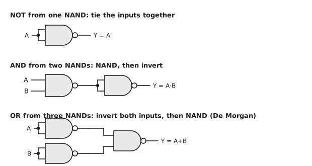
NOT. Tie both inputs of a NAND to the same signal:
$$\text{NAND}(A, A) = \overline{A \cdot A} = \overline{A}$$
by the idempotent law $A \cdot A = A$. One NAND with tied inputs is an inverter. It costs 4 transistors instead of the 2 of a real inverter, but it works.
AND. AND is NAND followed by NOT, and we now have NOT:
$$\text{NAND}(\text{NAND}(A,B),\ \text{NAND}(A,B)) = \overline{\overline{AB}} = AB$$
Two NANDs, 8 transistors. A real AND2 cell is 6 (a NAND plus a proper inverter), so we are not far off.
OR. This one uses De Morgan’s law, $A + B = \overline{\overline{A} \cdot \overline{B}}$. Invert A, invert B, and NAND the results:
$$\text{NAND}(\overline{A}, \overline{B}) = \overline{\overline{A} \cdot \overline{B}} = A + B$$
Three NANDs, 12 transistors.
| Function | NAND implementation | Gates |
|---|---|---|
| NOT(A) | NAND(A, A) | 1 |
| AND(A, B) | NAND(NAND(A,B), NAND(A,B)) | 2 |
| OR(A, B) | NAND(NAND(A,A), NAND(B,B)) | 3 |
Since {NOT, AND, OR} is a complete set, NAND alone is universal.
The same for NOR
NOR follows the same pattern with the dual De Morgan identity. Figure 2 shows the constructions.
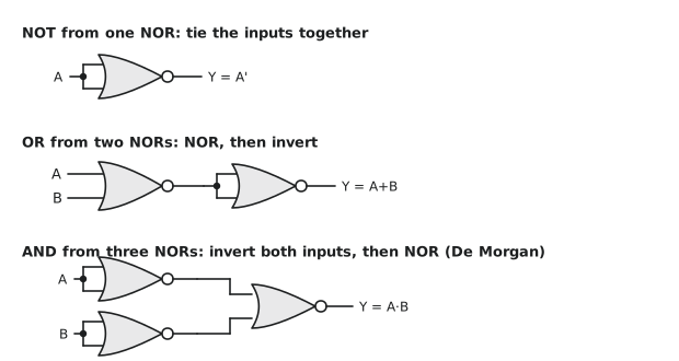
NOT is a NOR with tied inputs: $\text{NOR}(A, A) = \overline{A + A} = \overline{A}$. OR is a NOR followed by that inverter, two gates. AND uses De Morgan, $A \cdot B = \overline{\overline{A} + \overline{B}}$: invert both inputs and NOR them, three gates.
Why this matters in CMOS
Universality would be a curiosity if it were only mathematics. It matters because of how CMOS is built.
A NAND2 is 4 transistors. An AND2 is 6, because the only way to build a non-inverting gate in CMOS is to build the inverting one and add an inverter. The same holds for NOR and OR. The library gives you AND2 and OR2 cells for convenience, but inside they are NAND2 + INV and NOR2 + INV.
So when a synthesis tool has a function to implement, it prefers the inverting gates and tries to get rid of the extra inverters. The main trick for this is called bubble pushing: using De Morgan to move an inversion from the output of one gate to the inputs of the next, where it can often be absorbed. A chain of AND-OR logic turns into a chain of NANDs with no inverters at all, which is smaller and faster.
There is a historical angle too. Early gate arrays were built from one repeated tile that could be wired as a NAND or a NOR, and universality is what made a single tile type sufficient. More practically today, the internal representation inside a logic synthesizer is often a NAND network (or an and-inverter graph, which is the same idea), precisely because one gate type is enough to represent everything.
Converting a sum of products to NAND-NAND
Here is the practical technique. Given a sum-of-products expression, you can implement it as a two-level network of NAND gates without any other transformation. Take
$$F = AB + CD + E$$
The obvious implementation is two ANDs feeding a 3-input OR. Apply De Morgan to the whole thing:
$$F = AB + CD + E = \overline{\overline{AB} \cdot \overline{CD} \cdot \overline{E}}$$
The inner terms $\overline{AB}$ and $\overline{CD}$ are NANDs. The outer expression is a NAND of those results. Figure 3 shows both forms side by side.
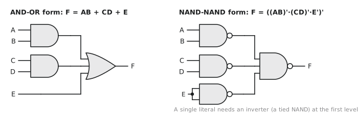
Note what happens to the single literal E. In the AND-OR form it goes straight into the OR. In the NAND-NAND form it must arrive at the second level already inverted, so it needs an inverter (a tied NAND) at the first level, or you use $\overline{E}$ directly if it happens to be available from elsewhere.
The way to remember it: the first level of NANDs computes the product terms (each one inverted), and the second-level NAND both undoes those inversions and performs the OR, because a NAND of inverted terms is an OR of the terms. Any SOP expression maps onto this structure directly.
The dual holds for product-of-sums expressions and NOR-NOR networks:
$$F = (A+B)(C+D) = \overline{\overline{(A+B)} + \overline{(C+D)}}$$
First-level NORs compute the sum terms, the second-level NOR does the AND. When a function’s POS form is smaller than its SOP form, the NOR-NOR implementation is the cheaper one, and synthesis tools evaluate both.
The 7400
I cannot write about NAND without mentioning the SN7400, Texas Instruments’ quad 2-input NAND chip from 1966. Four independent NAND gates in a 14-pin DIP package, TTL, 5 V supply, around 10 ns per gate.
The 7400 was one of the first digital ICs cheap enough for ordinary engineers to use in quantity. Before it, digital logic meant discrete transistors and resistors, hand-wired. Because NAND is universal, a drawer of 7400s could build any logic function you liked, and the part spawned the whole 7400 series: 7402 quad NOR, 7404 hex inverter, 7408 quad AND, 7474 dual D flip-flop, 7483 4-bit adder, and eventually thousands of part numbers that were the building blocks of digital electronics for two decades.
A nice example of single-gate design from the same era is the Apollo Guidance Computer. It was built almost entirely from one IC type, a dual 3-input NOR gate from Fairchild, several thousand of them. NOR is universal, and that is all they needed.
You can still buy the 74HC00, the CMOS version of the 7400, for a few cents. If you want to try this stuff by hand, a couple of 74HC00 chips and a breadboard are a complete logic lab.
Practice Exercise
Convert $F = A’B + AB’C$ to an all-NAND implementation. Try it before opening the solution.
Solution
The expression is already a sum of products with two terms, $A’B$ and $AB’C$.
The first level needs one NAND per product term. The first term contains $A’$, so we need an inverter on A (a NAND with tied inputs), and the second term needs $B’$ in the same way.
Term 1: a NAND2 with inputs $A’$ and $B$, giving $\overline{A’B}$.
Term 2: a NAND3 with inputs $A$, $B’$ and $C$, giving $\overline{AB’C}$.
The second level is a NAND2 of those two results:
$$F = \overline{\overline{A’B} \cdot \overline{AB’C}} = A’B + AB’C$$
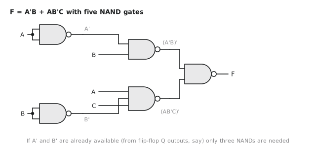
Figure 4 shows the circuit: two tied NANDs for the inverters, a NAND2, a NAND3 and the output NAND2, five gates in total. If $A’$ and $B’$ are already available, which is common when they come from flip-flops with both Q and Q̄ outputs, only three gates are needed.
In the next article we go one level down and look at what the transistors inside these gates are actually doing: how a CMOS inverter and a CMOS NAND are built, where the power goes, and why any of this matters to someone who only writes RTL.