The Seven Basic Gates
In the previous article we looked at what a gate is physically. In this one we go through the seven gates that every digital designer uses daily. If Boolean algebra is the grammar of digital design, these gates are the vocabulary, and you should know their truth tables well enough that you never have to look them up.
For each gate I give the symbol, the truth table, the Boolean expression, a typical use, and what it costs in CMOS transistors. At the end there is a comparison table you can come back to.
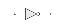
1. NOT gate (inverter)
| A | Y |
|---|---|
| 0 | 1 |
| 1 | 0 |
Boolean expression: $Y = \overline{A}$, also written $A’$ or $\neg A$.
Whatever goes in, the opposite comes out. You will use inverters for polarity changes everywhere: active-low reset signals, complementary clock phases, and inside nearly every larger gate.
Transistor count: 2, one PMOS pull-up and one NMOS pull-down. It is the simplest gate there is.
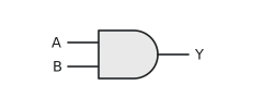
2. AND gate
| A | B | Y |
|---|---|---|
| 0 | 0 | 0 |
| 0 | 1 | 0 |
| 1 | 0 | 0 |
| 1 | 1 | 1 |
Boolean expression: $Y = A \cdot B$, usually just written $AB$.
The output is 1 only when every input is 1. The most common use is enable gating: data_out = data_in AND enable. When enable is LOW the data is blocked, when it is HIGH the data passes through. You will write this pattern hundreds of times.
Transistor count: 6. In CMOS an AND is built as a NAND (4 transistors) followed by an inverter (2 more). This is why synthesis tools prefer NAND to AND wherever they can get away with it.
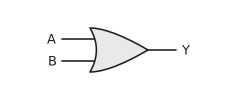
3. OR gate
| A | B | Y |
|---|---|---|
| 0 | 0 | 0 |
| 0 | 1 | 1 |
| 1 | 0 | 1 |
| 1 | 1 | 1 |
Boolean expression: $Y = A + B$.
The output is 1 if any input is 1. A typical use is interrupt aggregation: if any of several peripherals raises its interrupt line, the processor’s interrupt input goes HIGH. A few OR gates collect all the sources together.
Transistor count: 6, a NOR (4 transistors) followed by an inverter. Again the inverting version is the cheap one.
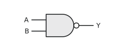
4. NAND gate
| A | B | Y |
|---|---|---|
| 0 | 0 | 1 |
| 0 | 1 | 1 |
| 1 | 0 | 1 |
| 1 | 1 | 0 |
Boolean expression: $Y = \overline{A \cdot B}$.
The output is LOW only when all inputs are HIGH; every other row is 1. Two cross-coupled NAND gates make an SR latch, the simplest memory element, which we will build in Module 3. NAND is also a universal gate, which gets its own article next.
Transistor count: 4. Two NMOS in series for the pull-down and two PMOS in parallel for the pull-up. This is the most efficient two-input gate in CMOS and the reason so much synthesized logic ends up as NAND trees.
5. NOR gate
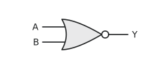
| A | B | Y |
|---|---|---|
| 0 | 0 | 1 |
| 0 | 1 | 0 |
| 1 | 0 | 0 |
| 1 | 1 | 0 |
Boolean expression: $Y = \overline{A + B}$.
The output is HIGH only when all inputs are LOW. A NOR across all the bits of a bus tells you when the bus is all zeros, which is exactly how the ZERO flag of an ALU is generated.
Transistor count: 4, the same as NAND, but with the topology swapped: two NMOS in parallel for the pull-down and two PMOS in series for the pull-up. The series PMOS is the weak point. PMOS is already the slower device, and putting two in series makes the pull-up slower still, so a NOR2 is typically slower than a NAND2 of the same size. Synthesis tools know this and lean towards NAND.
6. XOR gate
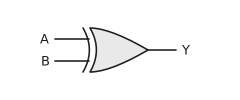
| A | B | Y |
|---|---|---|
| 0 | 0 | 0 |
| 0 | 1 | 1 |
| 1 | 0 | 1 |
| 1 | 1 | 0 |
Boolean expression: $Y = A \oplus B = A\overline{B} + \overline{A}B$.
The output is 1 when the inputs differ. XOR turns up in more places than any gate other than AND and OR, and it is worth knowing the main ones.
The first is the controllable inverter. Take $Y = A \oplus \text{ctrl}$. When ctrl is 0, $Y = A$ and the signal passes unchanged. When ctrl is 1, $Y = \overline{A}$ and the signal is inverted. Encryption, data scrambling and pseudo-random number generators all use XOR this way.
The second is addition. In a full adder the sum bit is $A \oplus B \oplus C_{in}$. Every adder you build starts from XOR.
The third is parity. The XOR of N bits is 1 when an odd number of them are 1. Figure 7 shows an 8-bit parity generator built from seven XOR gates arranged as a tree, three levels deep.
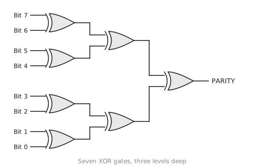
The fourth is CRC. The cyclic redundancy check used by Ethernet, USB and ZIP files is polynomial division in modulo-2 arithmetic, and modulo-2 arithmetic is nothing but XOR and shift registers.
Transistor count: 8 to 12 depending on the implementation. XOR cannot be built as a single pull-up/pull-down network the way NAND and NOR can, so it is more expensive, and large XOR trees are something to keep an eye on for both area and timing.
7. XNOR gate
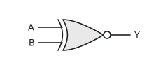
| A | B | Y |
|---|---|---|
| 0 | 0 | 1 |
| 0 | 1 | 0 |
| 1 | 0 | 0 |
| 1 | 1 | 1 |
Boolean expression: $Y = \overline{A \oplus B} = AB + \overline{A},\overline{B}$.
The output is 1 when the inputs match, so XNOR is an equality detector. To check whether two N-bit numbers are equal, XNOR each pair of bits and AND all the results:
A[7:0] == B[7:0]  is
  XNOR(A[7],B[7]) AND XNOR(A[6],B[6]) AND ... AND XNOR(A[0],B[0])
The AND output is HIGH only when every bit pair matches. This is how equality comparators inside an ALU work.
Transistor count: 8 to 12, the same as XOR. The extra inversion is usually absorbed into the cell.
The seven gates side by side
The columns 00, 01, 10 and 11 give the output for (A,B) = (0,0), (0,1), (1,0) and (1,1).
| Gate | Expression | 00 | 01 | 10 | 11 | Typical use |
|---|---|---|---|---|---|---|
| NOT | $\overline{A}$ | 1 | 0 | Inversion, active-low signals | ||
| AND | $AB$ | 0 | 0 | 0 | 1 | Enable gating, masking |
| OR | $A+B$ | 0 | 1 | 1 | 1 | Interrupt aggregation |
| NAND | $\overline{AB}$ | 1 | 1 | 1 | 0 | Universal gate, SR latch |
| NOR | $\overline{A+B}$ | 1 | 0 | 0 | 0 | Zero detection, universal gate |
| XOR | $A \oplus B$ | 0 | 1 | 1 | 0 | Adder sum, parity, scrambling |
| XNOR | $\overline{A \oplus B}$ | 1 | 0 | 0 | 1 | Equality comparison |
People mix up NAND with NOR, and XOR with XNOR, more often than you would expect. The quick check is that NAND and NOR are the complements of AND and OR, and XNOR is the complement of XOR. If you are unsure, start from AND or XOR and flip every output.
De Morgan’s laws, seen in the gates
Look at the AND/NAND and OR/NOR pairs in the table. De Morgan’s theorems from the last section state the relationship exactly:
$$\overline{A \cdot B} = \overline{A} + \overline{B}$$
$$\overline{A + B} = \overline{A} \cdot \overline{B}$$
In words, a NAND is an OR with inverted inputs, and a NOR is an AND with inverted inputs. This is not only algebra, it is a drawing convention. In a schematic you will often see an OR symbol with bubbles on its inputs. That is a NAND, drawn in the form that makes the designer’s intent clearer. When you see an AND with bubbles on the inputs, read it as NOR. Getting comfortable with these “De Morgan equivalent” symbols makes real schematics much easier to read.
Practice Exercise
Problem 1. Without looking at the tables above, construct the truth tables for NAND and XNOR from scratch. Use only AND and NOT to derive NAND, and only XOR and NOT to derive XNOR. Then check against the tables.
Solution
NAND is NOT(AND). Build the AND column first, then invert it:
| A | B | AND = AB | NAND = NOT(AB) |
|---|---|---|---|
| 0 | 0 | 0 | 1 |
| 0 | 1 | 0 | 1 |
| 1 | 0 | 0 | 1 |
| 1 | 1 | 1 | 0 |
XNOR is NOT(XOR). Build the XOR column (1 when the inputs differ), then invert it:
| A | B | XOR | XNOR |
|---|---|---|---|
| 0 | 0 | 0 | 1 |
| 0 | 1 | 1 | 0 |
| 1 | 0 | 1 | 0 |
| 1 | 1 | 0 | 1 |
Problem 2. Prove $\overline{A \cdot B} = \overline{A} + \overline{B}$ by building both truth tables and comparing them row by row.
Solution
| A | B | $\overline{A}$ | $\overline{B}$ | $A \cdot B$ | $\overline{A \cdot B}$ | $\overline{A} + \overline{B}$ |
|---|---|---|---|---|---|---|
| 0 | 0 | 1 | 1 | 0 | 1 | 1 |
| 0 | 1 | 1 | 0 | 0 | 1 | 1 |
| 1 | 0 | 0 | 1 | 0 | 1 | 1 |
| 1 | 1 | 0 | 0 | 1 | 0 | 0 |
The two bold columns are identical in every row, so the identity holds.
Problem 3. Describe the circuit you would build to detect whether an 8-bit bus equals 0xA5 (binary 10100101). Which gates would you use?
Solution
For each bit position where the target is 1 (bits 7, 5, 2 and 0), feed the bit straight into an XNOR with a constant 1, or simply use the bit as is. For each position where the target is 0 (bits 6, 4, 3 and 1), invert the bit first. Then AND all eight results. The AND output is HIGH only when every bit matches 10100101. In practice a synthesis tool would reduce this to one 8-input AND with inverters on the appropriate inputs.
In the next article we look at what real standard cell libraries add on top of these seven: multi-input gates, compound AND-OR-INVERT cells, tri-state buffers and transmission gates.