Multiplexers
Sections 1.1 to 1.4 gave us numbers, Boolean algebra, gates and a way to minimise logic. In this last section of Module 1 we assemble gates into the standard blocks that appear in nearly every design. We start with the multiplexer, because if you had to pick the single most common combinational block, this is it. It is in a processor’s bypass paths, in the routing fabric of an FPGA, in memory address selection, wherever a choice has to be made between two signals. And once you understand it, you understand what an FPGA lookup table is.
Selecting one of many
A multiplexer, or mux, is a data selector. It has $N$ data inputs $I_0 \ldots I_{N-1}$, $\log_2 N$ select lines, and one output $Y$. The select lines form a binary number, and the data input with that index is passed to the output. The other inputs are ignored. It is a railway switch: the trains wait on their own tracks and the position of the lever decides which one comes through.
The 2-to-1 mux
The simplest mux picks between two inputs with one select line.
| $S$ | $A$ | $B$ | $Y$ |
|---|---|---|---|
| 0 | 0 | 0 | 0 |
| 0 | 0 | 1 | 0 |
| 0 | 1 | 0 | 1 |
| 0 | 1 | 1 | 1 |
| 1 | 0 | 0 | 0 |
| 1 | 0 | 1 | 1 |
| 1 | 1 | 0 | 0 |
| 1 | 1 | 1 | 1 |
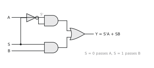
When $S = 0$, $Y$ follows $A$; when $S = 1$, $Y$ follows $B$. Reading the 1-rows as minterms and grouping by $S$:
$$Y = S’AB’ + S’AB + SA’B + SAB = S’A(B’ + B) + SB(A’ + A) = S’A + SB$$
This is the 2-to-1 mux equation and it is worth knowing by heart. Figure 1 shows the gate implementation: two AND gates, an OR gate and an inverter for $S’$.
The 4-to-1 mux
Two select lines choose among four inputs:
| $S_1$ | $S_0$ | $Y$ |
|---|---|---|
| 0 | 0 | $I_0$ |
| 0 | 1 | $I_1$ |
| 1 | 0 | $I_2$ |
| 1 | 1 | $I_3$ |
$$Y = S_1’S_0’,I_0 + S_1’S_0,I_1 + S_1S_0’,I_2 + S_1S_0,I_3$$
Each term says “when the selects point at this input, let it through”.
You do not need new hardware for a wider mux. Figure 2 builds a 4-to-1 mux from three 2-to-1 muxes: the first level reduces four inputs to two, the second level makes the final choice.
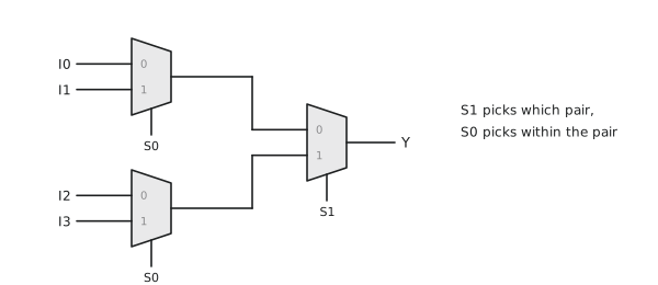
With $S_1 = 0$ the output mux passes the upper pair’s result, which is $I_0$ or $I_1$ according to $S_0$. With $S_1 = 1$ it passes the lower pair’s result, $I_2$ or $I_3$. The pattern continues: a $2^n$-to-1 mux needs $2^n - 1$ two-to-one muxes in $n$ levels.
| Mux | Select lines | Built from |
|---|---|---|
| 2-to-1 | 1 | gates |
| 4-to-1 | 2 | three 2-to-1 |
| 8-to-1 | 3 | three 4-to-1, or seven 2-to-1 |
| 16-to-1 | 4 | three 8-to-1 |
A mux can compute any function
This is the idea that connects the mux to the FPGA, so it is worth following carefully.
Take a 4-to-1 mux and connect the function’s variables $A$ and $B$ to the select lines. When $AB = 00$ the output is whatever is on $I_0$; when $AB = 01$ it is $I_1$, and so on. If each data input is tied to a constant 0 or 1, the mux implements whichever 2-variable function those four constants describe. That is every 2-variable function, from one mux and no gates.
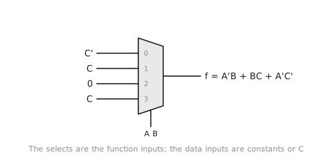
For a 3-variable function $f(A, B, C)$, use $A$ and $B$ as selects and connect each data input to $C$, $C’$, 0 or 1 as required. Take $f = A’B + BC + A’C’$. Split the truth table by $(A, B)$ and see what $f$ does as $C$ varies:
| $A$ | $B$ | $f$ at $C = 0$ | $f$ at $C = 1$ | Data input |
|---|---|---|---|---|
| 0 | 0 | 1 | 0 | $I_0 = C'$ |
| 0 | 1 | 0 | 1 | $I_1 = C$ |
| 1 | 0 | 0 | 0 | $I_2 = 0$ |
| 1 | 1 | 0 | 1 | $I_3 = C$ |
Wire $I_0 = C’$, $I_1 = C$, $I_2 = 0$, $I_3 = C$, and the mux implements $f$ (Figure 3).
The lookup table in an FPGA
An FPGA logic cell is built around a lookup table (LUT). A 4-input LUT holds 16 bits of configuration memory, one output bit for each of the $2^4$ input combinations. Those 16 bits are the data inputs of a 16-to-1 mux, and the four logic inputs are its select lines. For any input combination, the mux picks out the stored bit at that address.
That is a truth table implemented directly, and it means one 4-input LUT can implement any of the $2^{16} = 65{,}536$ functions of four variables. When you write assign y = a & b | c;, the synthesis tool computes the truth table and writes it into a LUT’s memory. Programming an FPGA is programming truth tables, not wires.
The routing between logic cells is also made of muxes. Each wire can connect to several others, and a routing mux configured at programming time picks which. The whole fabric is an array of logic muxes (the LUTs) and routing muxes. Placement chooses which LUTs to use, routing chooses how to set the routing muxes.
Where you will meet muxes
In a CPU, the outputs of the ALU, the load unit and the multiplier are muxed onto the write-back path to the register file, with the instruction’s opcode bits driving the select.
In a pipelined processor, an instruction may need a result that an earlier instruction has computed but not yet written back. Forwarding muxes at the input of each stage choose between the register file value and the result from a later stage. This is one of the densest concentrations of muxes in any processor.
Where several memory-mapped peripherals share a bus, the read data path back to the processor is usually a mux, with the address decoder driving the select.
Timing
A mux has a delay from its data inputs to its output and a separate delay from its select input to its output. If the select changes while the data inputs are stable, the output can glitch: for a moment during the select transition the mux may connect to neither, or briefly to the wrong, input. In combinational logic these glitches propagate.
People tend to assume the select is the slow signal and the data is what needs care. It is often the other way around, and in some designs (a clock-derived select in a DDR interface, for instance) the select changes fastest of all. The select-to-output path is a timing path like any other and shows up in timing reports like any other.
A worked example
Implement $f(A, B, C) = \sum m(0, 3, 5, 6)$ with a 4-to-1 mux, using $A$ and $B$ as selects.
| $A$ | $B$ | $C$ | $f$ |
|---|---|---|---|
| 0 | 0 | 0 | 1 |
| 0 | 0 | 1 | 0 |
| 0 | 1 | 0 | 0 |
| 0 | 1 | 1 | 1 |
| 1 | 0 | 0 | 0 |
| 1 | 0 | 1 | 1 |
| 1 | 1 | 0 | 1 |
| 1 | 1 | 1 | 0 |
Group by $(A, B)$:
| $A$ | $B$ | $f$ at $C = 0$ | $f$ at $C = 1$ | $I_i$ |
|---|---|---|---|---|
| 0 | 0 | 1 | 0 | $C'$ |
| 0 | 1 | 0 | 1 | $C$ |
| 1 | 0 | 0 | 1 | $C$ |
| 1 | 1 | 1 | 0 | $C'$ |
So $I_0 = C’$, $I_1 = C$, $I_2 = C$, $I_3 = C’$, $S_1 = A$, $S_0 = B$. This function is the 3-input XOR, which you can confirm from the table.
Practice Exercise
Problem 1. Implement $f = A \oplus B$ with a 2-to-1 mux. What goes on the data inputs?
Solution
Use $A$ as the select. When $A = 0$, $f = B$, so $I_0 = B$. When $A = 1$, $f = B’$, so $I_1 = B’$. One mux and one inverter.
Problem 2. A 4-to-1 mux has $I_0 = 1$, $I_1 = 0$, $I_2 = 1$, $I_3 = 0$. What is $Y$ when $S_1S_0 = 10$, and when $S_1S_0 = 01$?
Solution
$S_1S_0 = 10$ is index 2, so $Y = I_2 = 1$. $S_1S_0 = 01$ is index 1, so $Y = I_1 = 0$. (With these constants the mux computes $Y = S_0’$.)
Problem 3. Build an 8-to-1 mux from 4-to-1 muxes. How many are needed and how are they connected?
Solution
Two 4-to-1 muxes handle $I_0$ to $I_3$ and $I_4$ to $I_7$ respectively, both selected by $S_1S_0$. A 2-to-1 mux (or a third 4-to-1 with two inputs unused) selected by $S_2$ picks between their outputs. When $S_2 = 0$ the output comes from the lower group, when $S_2 = 1$ from the upper.
In the next article we look at the opposite operation: sending one signal to one of many destinations, which is the demultiplexer, and its close relative the decoder.