What a Logic Gate Really Is
In the last section we worked through Boolean algebra on paper. In this section we move from algebra to hardware. A logic gate is the physical device that computes a Boolean function, and the next four articles go through the gates you will use every day. Before that, I want to spend one article on what a gate actually is. A few physical facts about gates (they take time to switch, they can only drive so much, and the transistors inside them are not symmetric) explain most of the design rules you will meet later in this course.
A gate is a physical device
A logic gate takes one or more input voltages, computes a Boolean function of them, and drives the result onto its output as a voltage. The Boolean algebra of the previous section was pure mathematics. A gate is the point where that mathematics gets built out of silicon and starts doing work.
A modern CPU has more than ten billion gates in it. A large FPGA has hundreds of millions. Each one is simple: some inputs go in, one output comes out, following one fixed rule. Digital design is the business of stacking simple things together in the right order until you have something complicated.
The abstraction hierarchy
We do not think about electrons while writing Verilog, and we do not think about Verilog syntax while planning the architecture of a processor. Each level of a design hides what happens below it and presents a clean interface to the level above. Figure 1 shows the full stack, from the application down to the physics.
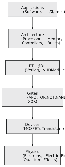
When you write assign y = a & b; you are working at the RTL level. The synthesis tool maps that line to a gate, an AND or more likely a NAND. Place and route maps the gate onto transistors from a standard cell library. The fabrication process turns those transistors into geometry on a wafer. Physics takes over from there.
For the whole of this course we will live at the RTL and gate levels. The reason for this article is to know enough about the levels underneath to make sensible decisions at the levels above. The hierarchy is also what lets a team of people design a chip with billions of transistors. You can reason about a module without knowing its transistor layout because the interface contract is clean. Respect the boundaries and they protect you. Break them carelessly and debugging becomes very hard.
CMOS in one paragraph
Nearly every gate you will ever use is built in CMOS, which stands for Complementary Metal-Oxide-Semiconductor. The building block is the MOSFET, a voltage-controlled switch, and it comes in two types.
An NMOS transistor conducts when its gate terminal is HIGH. NMOS transistors sit between the output and ground, so when they conduct they pull the output LOW. We call them pull-down devices.
A PMOS transistor conducts when its gate is LOW. PMOS transistors sit between the supply (VDD) and the output, so when they conduct they pull the output HIGH. These are the pull-up devices.
The “complementary” part means both types are used together, arranged so that in any stable state exactly one of the two networks conducts. There is never a direct path from VDD to ground, which is why a CMOS gate draws almost no current when it is not switching. That single property is why CMOS replaced TTL and NMOS-only logic in the 1980s.
The simplest CMOS gate is the inverter: one PMOS pull-up and one NMOS pull-down. Input HIGH turns the NMOS on and pulls the output to ground. Input LOW turns the PMOS on and pulls the output to VDD. Two transistors, and the behaviour is exactly complementary. Every standard cell library you will use, whether for an ASIC or inside an FPGA, is built on this structure. We will build a NAND gate out of transistors in the last article of this section.
Gates take time: propagation delay
This surprises most people the first time they hear it: a gate does not respond to its input instantly. The delay between an input changing and the output settling is called the propagation delay, written $t_{pd}$, and it is one of the hard limits on how fast a digital system can run.
There are actually two numbers per gate:
- $t_{pd,LH}$, the delay when the output goes from LOW to HIGH
- $t_{pd,HL}$, the delay when the output goes from HIGH to LOW
They differ because the pull-up network uses PMOS and the pull-down network uses NMOS, and the two are not equally fast. Electrons, the carriers in an NMOS channel, move through silicon faster than holes, the carriers in PMOS. So an NMOS transistor is faster than a PMOS transistor of the same size, and the output going LOW is usually the quicker transition. Designers compensate by making the PMOS devices about two to three times wider, but some asymmetry usually remains.
Some typical numbers, so you have a feel for the scale:
| Technology | Delay per gate |
|---|---|
| 5 nm CMOS | 15 to 30 ps |
| 28 nm CMOS | 50 to 100 ps |
| 180 nm CMOS | 200 to 500 ps |
| 7400-series TTL (1960s) | about 10 ns |
A picosecond is $10^{-12}$ seconds. The numbers look tiny, but a 5 GHz clock has a period of only 200 ps, so a chain of a handful of gates can use up an entire clock period.
Fan-in and fan-out
Two more physical limits decide how gates can be wired together.
Fan-in is the number of inputs a gate has. A 2-input AND has a fan-in of 2, a 4-input AND has a fan-in of 4. In CMOS, more inputs means more transistors in series (in the pull-down network of a NAND, or the pull-up network of a NOR). Transistors in series add resistance, so wide gates are slow. Standard cell libraries usually stop at four or six inputs and build anything wider out of a tree of smaller gates.
Fan-out is the number of gate inputs that one output drives. Each input is a small capacitive load. Connect eight inputs to one output and you have stacked eight capacitances, and the output now charges and discharges more slowly. Figure 2 shows the situation.
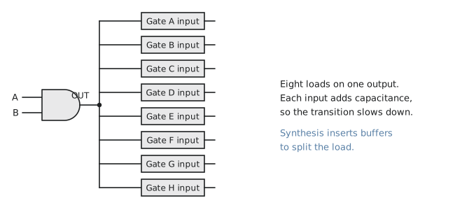
A fan-out of about four is a common guideline in standard cell design. A fan-out of eight is often acceptable with some timing penalty. A fan-out of thirty-two with no buffering would wreck the timing. In practice the synthesis tool inserts buffer trees whenever a net has to drive many loads. You will see these buffers appear in your netlists and wonder where they came from; this is where.
The critical path
Propagation delay, fan-in and fan-out all feed into one idea that runs through the rest of this course: the critical path. In any synchronous circuit, the critical path is the longest chain of gate delays between two flip-flops. It sets the minimum clock period, and therefore the maximum clock frequency:
$$f_{max} = \frac{1}{t_{critical_path} + t_{setup} + t_{clock_skew}}$$
Here $t_{setup}$ is the setup time of the destination flip-flop and $t_{clock_skew}$ allows for the clock arriving at slightly different times at different flip-flops. Both are covered properly in Module 3.
When a synthesis tool reports a timing violation, it is telling you that some path through your logic takes longer than the clock period allows. The fix is always one of three things: restructure the logic to reduce its depth, add a pipeline register to split the path, or slow the clock down.
A mistake I see often from people coming from software is the belief that combinational logic has no timing to worry about because “it is just logic”. It does. Everything between two registers has to finish within one clock cycle, and underestimating gate delay is one of the most common causes of timing trouble later on.
A worked example: an inverter chain
Figure 3 makes the delay concrete. Five inverters in a row, each with 100 ps of propagation delay, add up to 500 ps. If that chain sat between two flip-flops, it alone would limit the clock to 2 GHz. Now suppose the tool inserts a buffer of about 50 ps in the middle of the chain to fix a fan-out problem. The path is now 550 ps. Every element on the path counts.
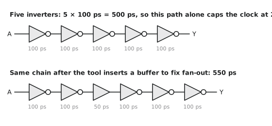
Real tools do this arithmetic with far more precision than my round numbers. They use delay models from the foundry, delivered as Liberty files and Standard Delay Format (SDF) files, that account for supply voltage, temperature and process variation. We will read such reports in the RTL to GDSII course.
Practice Exercise
- A path between two flip-flops passes through six gates of 80 ps each, plus one buffer of 40 ps. The destination flip-flop has a setup time of 30 ps and the clock skew budget is 20 ps. What is the maximum clock frequency for this path?
- A signal must drive 20 gate inputs, and the library guideline is a fan-out of 4. Sketch a buffer tree that meets the guideline. How many buffers does it need, and how many levels of delay does it add?
Solution
-
The path delay is 6 × 80 + 40 = 520 ps. Add the setup time (30 ps) and skew (20 ps) to get 570 ps. So $f_{max} = 1 / 570\text{ ps} \approx 1.75$ GHz.
-
One buffer can drive 4 loads, so 20 loads need 5 buffers at the last level. Those 5 buffers are themselves 5 loads, which is more than 4, so add a second level of 2 buffers driving 3 and 2 of them. The original signal drives those 2. That is 7 buffers and two extra levels of delay. A real tool would do something similar, and might use a larger-drive-strength buffer to save a level.
In the next article we go through the seven basic gates one at a time: the symbol, the truth table, the Boolean expression, what each one is used for, and what it costs in transistors.