De Morgan's Laws and Bubble Pushing
In the last article we went through the theorems of Boolean algebra. Two of them are used so much more than the rest that they deserve an article of their own. If you remember only two identities from this section, make them these:
$$(A \cdot B)’ = A’ + B’$$
$$(A + B)’ = A’ \cdot B’$$
These are De Morgan’s laws, named after Augustus De Morgan, who formalised them in 1847, the same year Boole published his algebra. They let you move between AND and OR, between positive and negative logic, and between what a gate does and what it means. You will use them when you read a schematic, when you simplify a complemented expression, when you work out why a circuit is mysteriously inverted, and when you try to understand why CMOS prefers NAND to AND. I want to show them three ways: by truth table, in plain English, and as a drawing technique.
Proof by truth table
With two variables there are four cases, so we check them all.
Law 1: $(A \cdot B)’ = A’ + B’$
| $A$ | $B$ | $A \cdot B$ | $(A \cdot B)'$ | $A'$ | $B'$ | $A’ + B'$ |
|---|---|---|---|---|---|---|
| 0 | 0 | 0 | 1 | 1 | 1 | 1 |
| 0 | 1 | 0 | 1 | 1 | 0 | 1 |
| 1 | 0 | 0 | 1 | 0 | 1 | 1 |
| 1 | 1 | 1 | 0 | 0 | 0 | 0 |
Law 2: $(A + B)’ = A’ \cdot B’$
| $A$ | $B$ | $A + B$ | $(A + B)'$ | $A'$ | $B'$ | $A’ \cdot B'$ |
|---|---|---|---|---|---|---|
| 0 | 0 | 0 | 1 | 1 | 1 | 1 |
| 0 | 1 | 1 | 0 | 1 | 0 | 0 |
| 1 | 0 | 1 | 0 | 0 | 1 | 0 |
| 1 | 1 | 1 | 0 | 0 | 0 | 0 |
The bold columns match in every row, so both laws hold. A truth table proves it but does not make it feel obvious, so here is the second way.
In plain English
Law 1 says “not (A and B)” is the same as “not A, or not B”. Put in words: “it is not true that both Alice and Bob came” means the same thing as “either Alice did not come, or Bob did not come, or neither did”. The NOT distributes onto each name, and the AND turns into OR.
Law 2 says “not (A or B)” is the same as “not A, and not B”. “Neither Alice nor Bob came” means “Alice did not come and Bob did not come”. To negate an OR, both things have to be false.
The rule to remember: when a NOT is pushed inside a bracket, it lands on every variable, and the operator flips. AND becomes OR, OR becomes AND. That is the whole of it.
In hardware: bubble pushing
This is where De Morgan turns from algebra into a daily skill. A NAND gate computes $(AB)’$. By Law 1 that is $A’ + B’$, which is an OR gate with both inputs inverted. In a schematic an inversion is drawn as a small circle, a bubble, on a pin. So the two symbols in the top row of Figure 1 are the same gate.
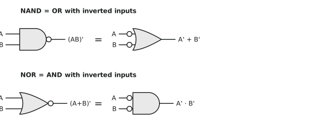
Likewise a NOR computes $(A + B)’$, which by Law 2 is $A’ \cdot B’$, an AND with inverted inputs.
Bubble pushing is the practice of redrawing a circuit with these equivalences so that it is easier to read, or so that it matches the gates you have. There are three rules:
- A bubble on the output of an AND can be moved to its inputs if the AND becomes an OR, and the other way round.
- A bubble on the output of an OR can be moved to its inputs if the OR becomes an AND, and the other way round.
- Two bubbles on the same wire cancel (involution).
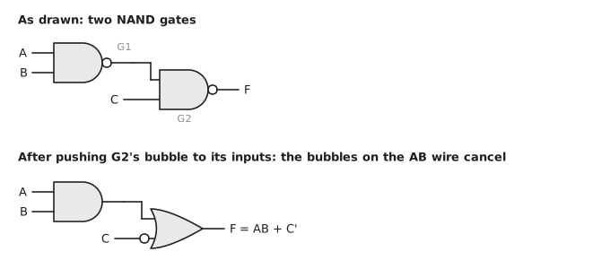
Figure 2 shows a two-level NAND circuit, and what it becomes after pushing the bubble of the second gate back to its inputs.
Algebraically:
$$F = ((AB)’ \cdot C)’ = ((AB)’)’ + C’ = AB + C’$$
After the push, G2 is an OR with bubbles on both inputs. The bubble on its upper input meets the bubble on G1’s output and the two cancel, leaving a plain AND. The bubble on the C input stays, so the function is $AB + C’$, which is much easier to read from the redrawn version than from the original.
In CMOS, NAND and NOR are the natural gates and AND and OR cost an extra inverter each, so real schematics and real netlists are full of bubbles. If you cannot push bubbles in your head, you cannot read them. This is not a textbook exercise; it is how the circuits are actually drawn.
More than two inputs
The laws extend to any number of variables:
$$(A \cdot B \cdot C)’ = A’ + B’ + C’$$ $$(A + B + C)’ = A’ \cdot B’ \cdot C’$$
or in general
$$\left(\prod_{i=1}^{n} A_i\right)’ = \sum_{i=1}^{n} A_i’ \qquad \left(\sum_{i=1}^{n} A_i\right)’ = \prod_{i=1}^{n} A_i’$$
“Not all three are 1” is “at least one is 0”. “None of the three is 1” is “all are 0”.
In Verilog the same identities hold for the bitwise operators:
// equivalent
assign F = ~(A & B & C);   // 3-input NAND
assign F = ~A | ~B | ~C;

// equivalent
assign G = ~(A | B | C);   // 3-input NOR
assign G = ~A & ~B & ~C;
Worked example 1: simplify $(AB’ + C)'$
Apply De Morgan to the outer NOT. The OR becomes AND and the NOT lands on each term:
$$(AB’ + C)’ = (AB’)’ \cdot C’$$
Apply De Morgan to $(AB’)’$. The AND becomes OR:
$$(AB’)’ = A’ + (B’)’ = A’ + B$$
Substitute back and expand:
$$F = (A’ + B) \cdot C’ = A’C’ + BC’$$
Spot check with $A = 0, B = 1, C = 0$. The original is $(0 \cdot 1 + 0)’ = 1$. The simplified form is $1 \cdot 1 + 1 \cdot 1 = 1$.
Worked example 2: NAND-NAND is AND-OR
Take two NAND gates, one with inputs A and B and one with inputs C and D, feeding a third NAND (Figure 3, left).
$$P = (AB)’ \qquad Q = (CD)’ \qquad F = (PQ)’ = ((AB)’(CD)’)’$$
Apply De Morgan to the outer NAND:
$$F = ((AB)’)’ + ((CD)’)’ = AB + CD$$
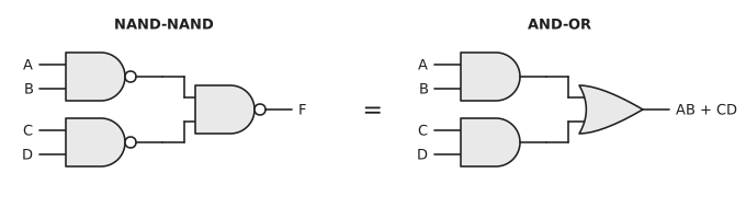
So two levels of NAND compute an AND-OR function. By the dual argument, two levels of NOR compute an OR-AND function. These two structures are what synthesis tools actually produce, because NAND and NOR are the cheap CMOS gates, and De Morgan is the reason they work. We come back to this in section 1.3 when we look at universal gates.
Why CMOS prefers NAND and NOR
A CMOS gate is built from two kinds of transistor. NMOS conducts when its gate is high, and PMOS conducts when its gate is low. The NMOS transistors form a pull-down network between the output and ground, the PMOS transistors form a pull-up network between the supply and the output, and the two networks are always duals of each other.
In a NAND gate the NMOS transistors are in series (both must be on to pull the output down) and the PMOS transistors are in parallel (either one pulls it up). The output is low only when both inputs are high, which is NAND. Four transistors, one stage.
An AND gate is a NAND followed by an inverter: six transistors and two stages. The extra stage costs delay, power and area, and across billions of gates it adds up. CMOS logic is inverting by nature, and De Morgan’s laws are what let you use that inversion instead of fighting it.
Practice Exercise
Problem 1. Simplify $(A + B’C)’$.
Solution
$$(A + B’C)’ = A’ \cdot (B’C)’ = A’ \cdot (B + C’) = A’B + A’C’$$
Problem 2. Prove that $(A \oplus B)’ = AB + A’B’$ using De Morgan’s laws. Recall that $A \oplus B = AB’ + A’B$.
Solution
$$(AB’ + A’B)’ = (AB’)’ \cdot (A’B)’ = (A’ + B)(A + B’)$$
Multiply out:
$$A’A + A’B’ + AB + BB’ = 0 + A’B’ + AB + 0 = AB + A’B’$$
which is XNOR. The complement of XOR is XNOR.
Problem 3. A circuit outputs $(A’B + C)’$. Use bubble pushing to find an equivalent using only AND and OR gates, with inverters allowed on the inputs.
Solution
$$(A’B + C)’ = (A’B)’ \cdot C’ = (A + B’) \cdot C’$$
Invert B, OR it with A, invert C, and AND the two results: two inverters, one OR and one AND.
In the next article we look at canonical forms, the mechanical way to write any truth table as a Boolean expression.