How CMOS Actually Works
This is the last article of the section on gates, and we go one level down, to the transistors. You will not lay out a transistor by hand anywhere in this course, and this is not a device physics article. There are no equations for channel current here. What I want to give you is enough of a picture of what sits underneath each Verilog statement that you can make sensible decisions about timing and power later on.
Every flip-flop you write in RTL becomes a small arrangement of inverters and pass gates. Every assign becomes a CMOS logic network. Every clock edge sets millions of these switches moving at once. It helps to know what they are.
The MOSFET as a voltage-controlled switch
A MOSFET (Metal-Oxide-Semiconductor Field-Effect Transistor) has three terminals that matter to us: gate, drain and source. The voltage on the gate decides whether the path between drain and source conducts. Almost no current flows into the gate, because the gate is insulated from the channel by a thin layer of oxide. That is what makes MOSFETs so good for logic: it costs almost nothing to make a control decision.
There are two types, shown in Figure 1.
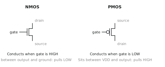
An NMOS transistor conducts when its gate is HIGH. Electrons carry the current, and electrons move through silicon faster than holes, so NMOS is the faster device. In a CMOS gate the NMOS transistors form the pull-down network between the output and ground.
A PMOS transistor conducts when its gate is LOW. Holes carry the current, and hole mobility is roughly half that of electrons, so a PMOS transistor has to be made wider to match the drive strength of an NMOS. In a CMOS gate the PMOS transistors form the pull-up network between VDD and the output.
The complementary arrangement is the whole point. In any steady state exactly one of the two networks conducts, so there is never a resistive path from VDD to ground. Older logic families such as NMOS-only logic had a load resistor permanently connected to VDD and drew current in one of the two output states all the time. CMOS got rid of that.
The CMOS inverter
The inverter is the simplest CMOS gate and the best one to understand first. It is one PMOS on top, source at VDD, and one NMOS underneath, source at ground. Both gates are tied to the input and both drains are tied to the output, as in Figure 2.
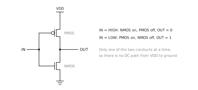
When the input is HIGH, the NMOS conducts and the PMOS is off, so the output is connected to ground and reads LOW. When the input is LOW, the PMOS conducts and the NMOS is off, so the output is connected to VDD and reads HIGH. That is an inverter.
In each stable state one transistor is fully on and the other fully off. The output is driven hard to one rail or the other, which is where CMOS gets its good noise margins, and no current flows once the output has settled.
There is one exception. While the input is crossing the middle of its swing, both transistors are partly on for a moment, and a short pulse of current flows straight from VDD to ground. This is called shoot-through or crowbar current. It only happens during transitions, but it is part of the reason switching costs energy.
A CMOS NAND gate
Now the 2-input NAND. Its output is LOW only when both A and B are HIGH:
| A | B | NAND |
|---|---|---|
| 0 | 0 | 1 |
| 0 | 1 | 1 |
| 1 | 0 | 1 |
| 1 | 1 | 0 |
The pull-down network has to connect the output to ground only when A = 1 and B = 1, so it is two NMOS transistors in series: both must conduct to complete the path. The pull-up network has to connect the output to VDD when A = 0 or B = 0, so it is two PMOS transistors in parallel: either one is enough. Figure 3 shows the circuit.
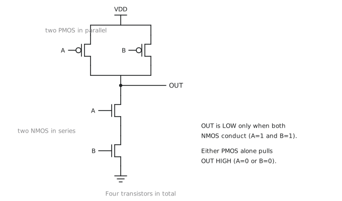
You can check every row of the truth table against the circuit:
| A | B | PMOS A | PMOS B | NMOS A | NMOS B | Path to VDD? | Path to GND? | OUT |
|---|---|---|---|---|---|---|---|---|
| 0 | 0 | on | on | off | off | yes | no | 1 |
| 0 | 1 | on | off | off | on | yes | no (series broken) | 1 |
| 1 | 0 | off | on | on | off | yes | no (series broken) | 1 |
| 1 | 1 | off | off | on | on | no | yes | 0 |
Four transistors, and in every row exactly one of the two networks conducts.
There is a general rule hiding here. Wherever the NMOS network has transistors in series, the PMOS network has them in parallel, and the other way round. NAND is series NMOS with parallel PMOS. NOR is parallel NMOS with series PMOS. Since PMOS is the slower device, the series PMOS stack in a NOR is what makes NOR slower than NAND, which is why synthesis tools reach for NAND first.
Where the power goes
CMOS power has two parts, and both follow directly from the transistor picture.
Static power
In steady state one network is off, and an ideal off transistor conducts nothing, so ideal CMOS dissipates no static power. This was the argument that won CMOS the market in the 1980s: a CMOS chip with its clock stopped draws essentially nothing.
Real transistors are not ideal. An off MOSFET still leaks a small subthreshold current, and at small geometries (roughly 28 nm and below, and badly below 10 nm) that leakage adds up to a significant fraction of the total power. Below about 65 nm the gate oxide also became thin enough, around a nanometre, for electrons to tunnel through it, which is a second leakage path. Managing leakage is a large part of the work at advanced nodes, though it is mostly invisible at the RTL level.
Dynamic power
Every time a node switches, energy is spent. When the output goes from 0 to 1, the PMOS network charges the load capacitance $C_L$ up to VDD. The energy drawn from the supply is $C_L V_{DD}^2$: half ends up stored in the capacitor and half is dissipated as heat in the PMOS resistance. When the output goes back to 0, the NMOS network discharges the capacitor and the stored half is dissipated too. So one full 0→1→0 cycle costs $C_L V_{DD}^2$.
Average that over a clock frequency $f$, with an activity factor $\alpha$ for the fraction of cycles in which the node actually switches, and you get the equation that every discussion of digital power comes back to:
$$P_{dynamic} = \alpha \cdot C_L \cdot V_{DD}^2 \cdot f$$
Each variable is something a designer can act on:
| Variable | Meaning | How it is controlled |
|---|---|---|
| $\alpha$ | Activity factor, 0 to 1 | Clock gating, operand isolation, pipeline enables |
| $C_L$ | Load capacitance | Shorter wires, smaller transistors, lower fan-out |
| $V_{DD}$ | Supply voltage | Voltage scaling, newer process nodes |
| $f$ | Clock frequency | Run slower where you can |
The square on $V_{DD}$ is why every new process node has lowered the supply voltage. Going from the 5 V of 1990s TTL to the 1 V of a modern node cuts dynamic power by a factor of 25 before counting anything else.
Moore’s law and the power wall
Gordon Moore observed in 1965 that the number of transistors on a chip doubled roughly every two years, and the trend held for over fifty years, driven by shrinking the transistors. Robert Dennard’s scaling rules from 1974 added the important part: as transistors shrink, VDD can shrink in proportion, and power density stays constant. For thirty years, smaller transistors were also lower-power transistors.
That stopped working around 2005. Below about 90 nm, leakage grew quickly, and VDD could no longer be reduced in step because the threshold voltage could not be lowered without making leakage worse still. Power density started rising with each node. Pushing the clock faster now meant more dynamic power on top of a leakage floor that was already significant, and mainstream clock frequencies stalled at 3 to 4 GHz around 2004.
The industry’s answer was to go wide instead of fast. The extra transistors went into more cores at moderate frequency rather than one core at a higher one. Figure 4 summarises the story.

What this means for RTL
If synthesis handles the transistors, why should an RTL designer care? Because $\alpha$ in $P = \alpha C V^2 f$ is set by the RTL, and power is very often the binding constraint on a design.
Clock gating
A flip-flop that is clocked but does not need to change still burns dynamic power in its clock network, and every output that toggles for no reason burns more in the logic it feeds. Clock gating puts an AND-like cell in front of the clock of a register bank so that when the block is idle, the clock stops. The activity factor for that block drops to nearly zero.
Modern synthesis tools infer clock gating from an enable condition in the RTL:
always_ff @(posedge clk) begin
    if (mul_en) result <= a * b;
    // else: result holds, and the tool can gate the clock on mul_en
end
Writing registers with an explicit enable is what makes this possible. Designs with thorough clock gating commonly save 30 to 50 percent of their dynamic power.
Operand isolation
Even when a result register is clock-gated, the combinational logic in front of it may still be toggling, because its inputs are still changing. A multiplier that is not being used will still ripple glitches through its adder tree every time an operand changes. Operand isolation forces the inputs to a constant when the block is idle:
// inputs toggle even when the product is unused
assign product = a * b;

// hold the inputs at zero when idle
assign a_gated = mul_en ? a : '0;
assign b_gated = mul_en ? b : '0;
assign product = a_gated * b_gated;
Constant inputs mean nothing inside the multiplier switches. The cost is a row of AND gates on the inputs, which is small next to the multiplier.
Pipeline enables
When a pipeline stalls, the stalled stages should hold their values rather than clock in whatever happens to be on their inputs:
always_ff @(posedge clk) begin
    if (stage_enable) begin
        data_reg <= data_in;
        ctrl_reg <= ctrl_in;
    end
end
This is the same enable pattern as before, applied stage by stage. In a processor that stalls often it recovers a good fraction of the power.
One habit to avoid is writing registers with no enable at all and trusting the tool to work out when they could be gated. In simple cases it will. In complicated ones it will not, and the power is gone. Write the enables explicitly and treat power as a design requirement rather than something to look at after synthesis.
Process corners
One last thing worth naming before we leave the transistor level. Manufacturing is not perfect, and transistors on different chips, or on different parts of one chip, have slightly different threshold voltages, oxide thicknesses and channel lengths. Foundries characterise the spread as process corners:
- FF (fast-fast): both NMOS and PMOS faster than nominal
- SS (slow-slow): both slower than nominal, the worst case for timing
- TT (typical-typical): nominal
- FS and SF: one device type fast and the other slow, the worst case for anything that depends on the balance between them
Timing sign-off has to pass at the SS corner, and leakage and power targets are checked at FF. As an RTL designer you meet this as a set of library files with different corner names, and as the reason the timing report you get at one corner is not the timing you get at another. We will use these libraries in the RTL to GDSII course.
Practice Exercise
Problem 1. Describe, in terms of the two switches, what happens in a CMOS inverter while the input goes from LOW to HIGH. Why does this cost energy even in ideal CMOS?
Solution
While the input is between the two rails, the NMOS is turning on and the PMOS is turning off, and for a short time both conduct. A pulse of shoot-through current flows from VDD to ground. Separately, the output capacitance has to be discharged through the NMOS, which dissipates the $\frac{1}{2} C_L V_{DD}^2$ that was stored when the output was last charged. Neither of these is leakage; they are the cost of changing state, and together they are what the dynamic power equation counts.
Problem 2. A block runs at 2 GHz with an activity factor of 0.3, a switched capacitance of 500 pF and a supply of 1.0 V. What is its dynamic power? What does it become if clock gating cuts the activity factor to 0.06?
Solution
$$P = \alpha C V_{DD}^2 f = 0.3 \times 500 \times 10^{-12} \times 1.0^2 \times 2 \times 10^9 = 0.3 \text{ W}$$
With $\alpha = 0.06$ the same calculation gives 60 mW. Clock gating saved 240 mW, an 80 percent reduction for that block.
Problem 3. Why is a NAND2 faster than a NOR2 with the same transistor sizes?
Solution
In a NAND2 the two PMOS pull-up transistors are in parallel and the two NMOS pull-down transistors are in series. In a NOR2 it is the other way round: parallel NMOS and series PMOS. PMOS is already the slower device, and putting two in series doubles the pull-up resistance, so the NOR’s rising output is slow. The NAND’s worst case is its series NMOS stack, but NMOS is the fast device, so the penalty is smaller. In most libraries a NAND2 is 10 to 30 percent faster than a NOR2 of the same size.
That completes the section on gates. In the next section we return to Boolean functions and look at Karnaugh maps, the graphical method for simplifying them before they ever become gates.