Decoders and Demultiplexers
In the previous article a multiplexer chose one of many inputs. In this one we go the other way. Every time a processor accesses memory, a decoder decides which chip or which peripheral the address belongs to. Every instruction that enters a processor is decoded to find out which unit should execute it. Decoders are quiet, fast, and in every system.
What a decoder does
A decoder takes an $n$-bit input and activates exactly one of its $2^n$ outputs. All the others stay low. Output $Y_i$ is 1 exactly when the input, read as a binary number, equals $i$. It is a sorting machine: the address on the envelope decides which one pigeonhole the letter goes into.
The 2-to-4 decoder
Inputs $A_1 A_0$, outputs $Y_3$ to $Y_0$. Ask when each output should be high. $Y_0$ is high only for input 00, that is $A_1 = 0$ and $A_0 = 0$, so $Y_0 = A_1’A_0’$. The same reasoning for the others gives:
$$Y_0 = A_1’A_0’ \qquad Y_1 = A_1’A_0 \qquad Y_2 = A_1A_0’ \qquad Y_3 = A_1A_0$$
| $A_1$ | $A_0$ | $Y_3$ | $Y_2$ | $Y_1$ | $Y_0$ |
|---|---|---|---|---|---|
| 0 | 0 | 0 | 0 | 0 | 1 |
| 0 | 1 | 0 | 0 | 1 | 0 |
| 1 | 0 | 0 | 1 | 0 | 0 |
| 1 | 1 | 1 | 0 | 0 | 0 |
Figure 1 shows the circuit: two inverters and four AND gates, each AND taking the right true or complemented version of each input.
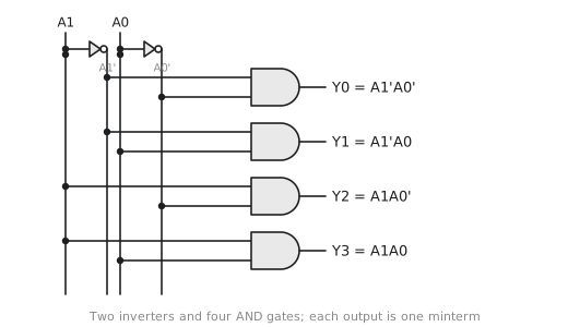
Look at those four expressions again. They are the minterms $m_0$ to $m_3$ of $A_1$ and $A_0$. A decoder is a minterm generator: each output is exactly one minterm of the inputs. That observation is what makes the next two sections work.
The enable input
Real decoders have an enable input, EN. When EN is low all outputs are forced low whatever the address; when EN is high the decoder works normally.
| EN | $A_1$ | $A_0$ | $Y_3$ | $Y_2$ | $Y_1$ | $Y_0$ |
|---|---|---|---|---|---|---|
| 0 | X | X | 0 | 0 | 0 | 0 |
| 1 | 0 | 0 | 0 | 0 | 0 | 1 |
| 1 | 0 | 1 | 0 | 0 | 1 | 0 |
| 1 | 1 | 0 | 0 | 1 | 0 | 0 |
| 1 | 1 | 1 | 1 | 0 | 0 | 0 |
Each output becomes $Y_i = EN \cdot m_i$, one more input on each AND gate.
The chip-select pin on a memory device is exactly this enable. The upper address bits are decoded into chip selects, the selected chip responds, and every other chip stays off the bus.
A decoder implements any function
Since every output is a minterm, any function of the inputs is an OR of some outputs. To implement $f(A_1, A_0) = \sum m(1, 2, 3)$, connect $Y_1$, $Y_2$ and $Y_3$ to an OR gate. The decoder makes the minterms; you pick the ones you want.
It gets more useful with several functions at once. With one decoder and two OR gates:
$$f_1 = \sum m(0, 3) = Y_0 + Y_3 \qquad f_2 = \sum m(1, 2) = Y_1 + Y_2$$
This is how early read-only memories were built: a decoder selects a row, and an OR plane on each output bit holds the stored pattern. A ROM is a decoder with a programmable OR array behind it.
Building a 3-to-8 decoder from two 2-to-4 decoders
The enable input is what makes decoders stackable. To decode three bits $A_2 A_1 A_0$ into eight outputs, split the outputs into two groups of four. Feed $A_1 A_0$ to both decoders. Enable the lower decoder (outputs $Y_0$ to $Y_3$) with $A_2’$ and the upper decoder ($Y_4$ to $Y_7$) with $A_2$, as in Figure 2.
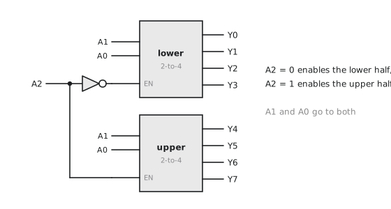
With $A_2 = 0$ only the lower decoder is enabled and $A_1 A_0$ picks one of $Y_0$ to $Y_3$. With $A_2 = 1$ only the upper one is enabled and $A_1 A_0$ picks one of $Y_4$ to $Y_7$. The same step turns two 3-to-8 decoders into a 4-to-16, and so on.
The demultiplexer
A demultiplexer (demux) is the routing opposite of a mux. A mux takes many inputs to one output; a demux takes one data input to one of many outputs, chosen by the select lines.
A decoder with an enable input is a demux. Rename EN as the data input $D$:
$$Y_i = D \cdot m_i(\text{select lines})$$
When $D = 1$ the selected output goes high; when $D = 0$ every output stays low. The data has been routed to the selected output. The two devices are the same circuit, and the difference is only what you use it for. Manufacturers sometimes sell one part under both names.
Address decoding
A concrete example. Suppose a 64 KB address space is split into four 16 KB regions, each served by its own memory chip:
| Chip | Address range |
|---|---|
| 0 | 0x0000 to 0x3FFF |
| 1 | 0x4000 to 0x7FFF |
| 2 | 0x8000 to 0xBFFF |
| 3 | 0xC000 to 0xFFFF |
A 16-bit address has bits A15 to A0. The top two bits identify the region: 00 is chip 0, 01 is chip 1, and so on. So A15 and A14 go into a 2-to-4 decoder, and its four outputs are the four chip selects. The lower 14 bits go to every chip in parallel and address a location within it; only the chip whose select is active responds. Figure 3 shows the arrangement.
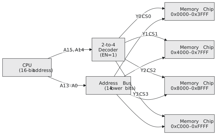
Microcontroller memory maps are built this way. On an STM32 the top few address bits pick the bus (AHB or APB), and a tree of decoders fans out from there to individual peripherals.
A worked example: 4-to-16 from two 3-to-8
Two 3-to-8 decoders each have inputs $A_2 A_1 A_0$ and an enable. To make a 4-to-16 decoder with inputs $A_3 A_2 A_1 A_0$, feed $A_2 A_1 A_0$ to both, enable the lower one with $A_3’$ and the upper one with $A_3$.
| $A_3$ | $A_2$ | $A_1$ | $A_0$ | Active output |
|---|---|---|---|---|
| 0 | 0 | 0 | 0 | lower $Y_0$ |
| 0 | 1 | 1 | 0 | lower $Y_6$ |
| 1 | 0 | 0 | 1 | upper $Y_9$ |
| 1 | 1 | 1 | 1 | upper $Y_{15}$ |
One inverter and two decoders.
Practice Exercise
Problem 1. Using one 2-to-4 decoder and OR gates, implement $f_1 = A \oplus B$ and $f_2 = A \odot B$ at the same time.
Solution
XOR is 1 when the inputs differ, rows 1 and 2, so $f_1 = Y_1 + Y_2$. XNOR is 1 when they match, rows 0 and 3, so $f_2 = Y_0 + Y_3$. Two OR gates. As expected, $f_2 = f_1’$.
Problem 2. A 32 KB memory space is divided into eight 4 KB regions. How many address bits are there, how many select the region, and what decoder is needed?
Solution
32 KB is $2^{15}$ bytes, so 15 address bits, A14 to A0. Eight regions need 3 bits, A14, A13 and A12, into a 3-to-8 decoder whose outputs are the eight chip selects. The remaining 12 bits address within a 4 KB region.
Problem 3. A mux drives one end of a serial link and a demux receives the other end, both with their select lines driven by the same counter. What does the system do?
Solution
The mux puts each of its $N$ inputs on the link in turn, one per count. The demux, stepping through the same sequence, routes each time slot to the matching output. $N$ signals travel over one wire, separated in time. This is time-division multiplexing, and it is the basis of much of telephony and of some I/O expansion schemes.
In the next article we look at the reverse of decoding, the encoder, and at the priority encoder, which deals with the real situation of several inputs being active at once.