The Antenna Effect, Explained Physically
In Section 8.2 we checked that the layout implements the right circuit. In this section we look at a failure that sounds impossible at first: the chip can be damaged by its own wiring before it has finished being built. Not during test, not in the field, but during fabrication, while one of the metal layers is being etched. This is the antenna effect. DRC and LVS are both blind to it, because it is not a geometry problem or a connectivity problem. It is a process physics problem.
The mechanism
A chip is built one layer at a time, and each metal layer is patterned by plasma etching: the wafer sits in an ionised gas that removes the metal you do not want and leaves the wires you do. During that step the exposed metal collects electrical charge from the plasma.
Normally the charge has somewhere harmless to go. A wire that is connected, through the layers already built, to a diffusion region (a transistor’s source or drain, or a diode) can bleed charge into the substrate. The danger is a piece of metal that, at that point in the process, is connected to a transistor gate and to nothing else. The route to the driver’s diffusion may only be completed by a later layer. Until then, the charge on that metal has one place to go: across the gate oxide.
A MOSFET’s gate oxide is only a few nanometres thick. Under normal operating voltages it is an excellent insulator, but enough accumulated charge raises the field across it until current is forced through the oxide by tunnelling. Depending on how much charge builds up, the result is either immediate breakdown of the oxide, or a smaller amount of damage that does not show as a defect on day one but shortens the transistor’s life and shows up as a reliability failure months or years later. Figure 1 shows the situation.
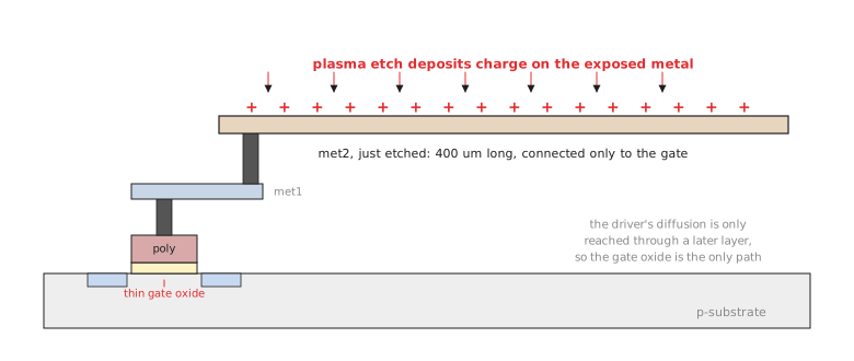
The key phrase is “connected to the gate and nothing else”. The moment the net reaches a diffusion, the discharge path exists and the risk for that net is over. But the check has to be made layer by layer. A net that is a short, harmless met1 stub while met1 is etched can be dangerous while met2 is etched, if a long met2 run joins the gate before anything joins it to a diffusion.
I have written about this mechanism separately, with more detail on the physics and on how it changes at smaller process nodes, in the antenna diode article on this site. It makes a good companion to this section.
Quantifying the risk: the antenna ratio
The risk is not just “is the net long”. It is the ratio between how much metal collects charge and how much gate oxide has to absorb it:
$$ \text{Antenna ratio} = \frac{\text{Area of metal connected to the gate}}{\text{Area of the gate oxide}} $$
The rule deck sets a maximum ratio for each layer, and a net that exceeds it is flagged. Two details matter in practice. The “metal area” is defined by the rule: for SKY130’s metal layers it is the wire’s sidewall area (perimeter times thickness), since the sidewalls are where most of the charge is collected, while other layers use the top area. And the limit can depend on how much diffusion is connected to the net, because diffusion provides a discharge path. The exact limits are in the PDK’s rules and the technology LEF; the relationship is what matters for intuition. More metal on one small gate means more charge concentrated on the same small piece of oxide.
For a feel for the arithmetic, take an illustrative met2 net with 40 µm² of metal area wired to a minimum-size gate with 0.05 µm² of oxide area:
$$ \text{Ratio} = \frac{40}{0.05} = 800 $$
Whether 800 passes depends entirely on the process’s limit, which is why this is checked by a tool against the real rules rather than judged by eye. The lab in two articles does exactly that.
Which net is riskier?
This is the reasoning to practise before you run a real checker. Two nets each drive a gate of similar, minimum size:
- Net A: a 2 µm met1 segment connecting two neighbouring cells.
- Net B: a 900 µm net crossing most of the die on met3, from a clock buffer to a distant gate.
Net B is far riskier, for two reasons that add up. More length means more metal area exposed to the plasma on every layer the net uses, which raises the numerator of the ratio. And a long net usually crosses several layers, so it is exposed at several etch steps. Net A reaches its driver’s diffusion almost immediately and collects very little.
A mistake I see is treating antenna risk as something checked once, on the finished net. It is evaluated per layer. For each metal layer, the check looks at the metal of that layer which is connected to the gate at the moment that layer is etched, the partial ratio, and SKY130 also checks a cumulative ratio that adds up the partial ratios of the layers below. A net that is clean at met1 can still fail at met3.
Hands-on: estimate the risk by hand
A net has three pieces of metal connected to one gate before anything connects it to a diffusion: 15 µm² on met1, 60 µm² on met2 and 25 µm² on met3 (using whatever area measure the rule defines). The gate oxide area is 0.08 µm². The cumulative ratio at met3 counts all three:
$$ \text{Cumulative ratio} = \frac{15 + 60 + 25}{0.08} = \frac{100}{0.08} = 1{,}250 $$
The partial ratio for met2 alone would be 60 / 0.08 = 750. That is the shape of a real antenna check: add up the relevant metal area layer by layer, divide by the gate area, and compare with the limits. The tool in the lab does exactly this for every net and every layer.
Practice Exercise
Two nets end on gates with the same oxide area. Net X has 30 µm² of met1 and nothing else. Net Y has 10 µm² of met1, 8 µm² of met2 and 6 µm² of met3, all connected to the gate before it reaches any diffusion. Which net has the higher partial ratio on its worst layer, and why might that surprise someone thinking only in terms of total metal?
Solution
Net X. Its worst layer is met1 with 30 µm². Net Y’s worst layer is also met1, with only 10 µm², and its met2 and met3 partial ratios are smaller still. So Net X’s worst partial ratio is three times Net Y’s, even though their total metal is not very different (30 against 24 µm²) and Net Y is the longer, more spread-out net.
This is the counter-intuitive part: “longer net” and “worse antenna ratio” are related but not the same thing. A short net with a lot of metal concentrated on one layer can fail a partial-ratio check that a longer, more spread-out net passes. The cumulative check narrows the gap, since Net Y’s total of 24 µm² is counted at its top layer, but the partial checks treat each layer separately.
In the next article we look at the two standard fixes, antenna diodes and jumpers, and when a flow prefers one over the other.