Why Chemical-Mechanical Polishing Needs Metal Fill
Every check so far in this module exists because the layout could be wrong in some electrical or geometric way. This last section is different. Metal fill does not fix anything in your design. It adds shapes with no electrical function at all, purely because the manufacturing process needs them. In this article we look at why a process step gets to dictate part of your layout, and clear up a confusion about the word “fill” that trips up a lot of people.
What CMP does
After each metal layer is patterned and the insulating dielectric is deposited over it, the wafer surface is not flat. It follows the shapes underneath. Before the next layer can be patterned accurately, the surface has to be flattened again, because lithography needs a flat, predictable focal plane. On an uneven surface, parts of the next layer’s pattern are in focus and parts are not.
Chemical-mechanical polishing (CMP) does the flattening: a rotating pad and a chemical slurry grind and dissolve the surface back to flat before the next layer goes on.
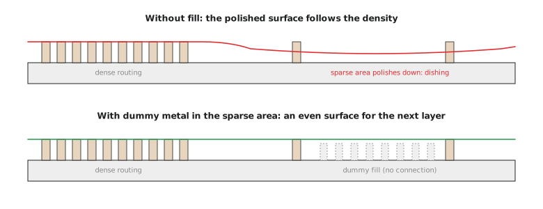
Here is where your layout comes in. The polishing rate depends on the local density of what is being polished. Metal and dielectric polish at different rates, and a region packed with metal behaves differently from a region with a few thin wires and lots of empty space. Polish a wafer with very uneven density and the sparse regions are polished down further than the dense ones, an effect called dishing or erosion. That brings back the unevenness CMP was meant to remove, and it also changes the thickness of the metal, and so its resistance, from place to place. Figure 1 shows the idea.
Metal fill: metal with no job
The fix is very direct. Wherever a region of a layer is too sparse, add extra metal shapes to bring its density up into the allowed range. These shapes are not connected to anything. They carry no signal and no power, and as far as your netlist is concerned they do not exist. Their only job is to occupy area on that layer so that CMP sees a more uniform surface.
Because fill has to be judged against the final content of every layer, it is one of the very last things added to the layout, after routing and after the checks in this module. Adding it any earlier would mean measuring density against geometry that is still going to change. In the SKY130 open shuttle programs, metal fill was typically generated at tapeout by the shuttle’s own scripts over the whole chip, which is one reason designs submitted to them had to leave the layout free of anything that would stop fill being placed.
Fill is not invisible to the other checks. The shapes are real geometry, so DRC is run again after fill. They also add a little capacitance to nearby wires, which is why careful flows either keep fill a set distance from sensitive nets or include it in the final extraction.
Filler cells are something else
This is the confusion I mentioned. OpenLane has a step called fill insertion, and the SKY130 library has cells called sky130_fd_sc_hd__fill_1, fill_2, fill_4 and fill_8. These are not metal fill for CMP.
Filler cells go into the standard cell rows, into the gaps between logic cells that placement left empty. They keep the n-well, the implant layers and the met1 power rails continuous along the row, which the process rules require. Decap cells (decap_3, decap_4 and so on) do the same job while also adding decoupling capacitance between the supply rails. Both kinds are proper cells in the netlist, placed by OpenLane.
Metal fill is loose dummy shapes on the routing layers, not cells, not in the netlist, added to the GDS at the very end. Both are called “fill”, they solve different problems, and they live at different points in the flow. We will see both on the UART in the lab.
Hands-on: look at a real filler cell
Look at how the library defines a filler cell:
grep -A25 "MACRO sky130_fd_sc_hd__fill_1" \
  "$PDK_ROOT/sky130A/libs.ref/sky130_fd_sc_hd/lef/sky130_fd_sc_hd.lef"
You will find a cell with a size, power pins (VPWR, VGND, VPB, VNB), and nothing else: no signal pins, and in the Liberty file no timing arcs. Compare it with a logic cell’s LEF from Module 2. The difference shows that these cells exist to complete the rows, not to do any logic. Note also that it contains nothing on met2 and above, so it does nothing for the density of the routing layers. That job belongs to metal fill.
Practice Exercise
A colleague suggests skipping metal fill on a small test chip “since it’s just a prototype and yield does not matter much”. Given what CMP does, is that a good argument? What risk is being traded away?
Solution
It is weaker than it sounds. The risk from missing fill is not only that a few dies on the wafer fail. Uneven polishing can spoil the focus and the metal thickness in the affected regions for every layer built on top, which can produce real defects (opens, shorts, marginal connections) or resistances quite different from what extraction assumed, on any die, including the one you care about.
For a single prototype that is arguably worse, not better: there is no wafer full of dies to choose a good one from. And in practice the question often does not arise, because the foundry or shuttle program requires density rules to be met and adds fill itself. Fill’s costs, a little extra capacitance on nearby wires and some more data, are real but small and well understood. Skipping it trades them for a defect risk that is hard to quantify.
Adding metal “until it looks dense enough” is not how fill works in practice. It is governed by density rules with specific minimum and maximum values, and in the next article we look at how those rules are defined and checked.