Electromigration: Why Current Density Limits Exist
In the previous article we looked at IR drop, which is about voltage right now: does every cell get close enough to the intended supply with today’s current. Electromigration is a different kind of problem. It is about what sustained current does to the metal itself, slowly, over months and years of operation. A wire that passes the IR drop check comfortably can still fail years into a product’s life, which is why electromigration gets its own check.
What happens inside the wire
A metal wire carrying current is a lattice of metal atoms with a stream of electrons flowing through it. The electrons collide with the atoms as they go. At normal current densities this has no noticeable effect over any realistic time. But at high enough current density, sustained long enough, the collisions have a cumulative, directional effect: the electrons all flow the same way, so they push atoms the same way, and over time atoms move along the wire in the direction of electron flow.
That movement is not uniform, and it creates two kinds of damage, shown in Figure 1:
- Voids, where atoms have moved away. The wire thins locally until it can break, an open circuit.
- Hillocks, where atoms pile up. They can grow far enough to touch a neighbouring wire, a short.
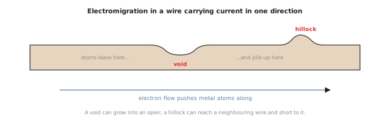
Like the slow oxide damage in the antenna section, this is a wear-out mechanism. It does not show as a defect on the tester. It shows as a field failure long after the chip passed every production test.
This is why electromigration is checked against current density, not current. 10 mA is only a problem if it is squeezed through a small cross-section. The same 10 mA through a much wider wire is fine. It is also why the direction of current matters. Power rails and straps carry current in one direction all the time, which is the worst case. Signal wires carry current back and forth as they charge and discharge, and the damage partly reverses, so their limits (expressed as RMS or peak current) are much more generous. For a digital design the main electromigration concern is the power grid and the vias in it.
Current density
$$ J = \frac{I}{A} $$
$J$ is the current density, $I$ the current and $A$ the cross-section of the wire: width times the metal thickness of that layer. Every process specifies the maximum allowed current density for each metal layer, and separately for vias, usually at a stated temperature, because electromigration gets much faster as the metal gets hotter. PDKs often express the limit as current per micron of wire width for each layer, which is the same thing with the thickness folded in. The real SKY130 limits are in the PDK documentation. For the worked examples here I will use an illustrative 2.0 mA/µm².
Take a met1 power rail in a standard cell row, 0.48 µm wide, on a layer 0.36 µm thick:
$$ A = 0.48\ \mu m \times 0.36\ \mu m \approx 0.17\ \mu m^2 $$
$$ I_{max} = 2.0\ \frac{mA}{\mu m^2} \times 0.17\ \mu m^2 \approx 0.35\ mA $$
So one rail can carry about 0.35 mA of steady current before it reaches this limit. If a long row of busy cells draws more than that through one end of the rail, the fix is not exotic: connect the rail to the straps above more often, so the current has more, shorter paths and each piece of rail carries less.
Vias work the same way, but their cross-section is small and fixed, so the limit is usually given per via cut. This is why power connections in real layouts use arrays of vias, several cuts in parallel between the same two layers, instead of one. Each cut carries its share of the current and stays under its own limit.
Electromigration and IR drop side by side
| IR drop | Electromigration | |
|---|---|---|
| What it is | Voltage lost across grid resistance, now | Slow physical wear from sustained current density |
| When it shows | Immediately, as slower cells or failing timing | Gradually, as opens or shorts years into the product’s life |
| Fixed by | Wider or denser straps, more connections, lower resistance | Wider metal and more vias where current is concentrated, lower current density |
| Checked by | Static or dynamic IR drop analysis | Current density checks, often from the same analysis |
The fixes overlap a lot. A wider strap lowers resistance, which helps IR drop, and lowers current density for the same current, which helps electromigration. That is why the strap widths chosen in Module 3 were always doing two jobs at once.
Hands-on: check a strap against both limits
Take the met4 strap from the previous article: 4 µm wide, carrying 8 mA in a larger design. SKY130’s met4 is roughly 0.85 µm thick (check the PDK for the exact figure). With the illustrative 2.0 mA/µm² limit:
$$ A = 4\ \mu m \times 0.85\ \mu m = 3.4\ \mu m^2 $$
$$ J = \frac{8\ mA}{3.4\ \mu m^2} \approx 2.4\ \frac{mA}{\mu m^2} $$
That is over the illustrative limit, even though the same strap was comfortable for IR drop. Widening it to 5 µm gives 4.25 µm² and 1.9 mA/µm², just under the limit; 6 µm would leave proper margin. The point of the example is that the two checks are independent: a strap can be fine for voltage and still too narrow for the current it carries, or the other way round.
Practice Exercise
A via between two metal layers is allowed an illustrative 0.18 mA per cut. A point in the power grid must pass a steady 0.5 mA through this via position. Is one cut enough? If not, how many cuts in parallel are needed?
Solution
One cut carries at most 0.18 mA, well short of 0.5 mA.
Cuts needed: 0.5 / 0.18 ≈ 2.78, rounded up to 3.
Three cuts allow 3 × 0.18 = 0.54 mA, which covers 0.5 mA with a little room. In practice I would use four for margin, since the current is never shared perfectly evenly between cuts. This is where the via arrays in power grids come from: not a layout habit, but a direct consequence of per-via current limits.
So far we have done both checks by hand on single segments. In the next article we run a real IR drop analysis on the UART’s routed power grid.