Running Fill Insertion on the UART
In the last two articles we looked at why density matters and how the rules are written. In this article we deal with both kinds of fill on the UART, the filler cells in the rows and the metal density on the routing layers, then run DRC and LVS once more and sum up what the design has passed in this module.
Step one: filler and decap cells
In OpenLane, the step called fill insertion places filler and decap cells into every empty site left in the standard cell rows. In the current OpenLane flow it runs just after detailed routing (older versions ran it just before). Since these cells contain only the row’s wells, implants and rails, they can go under the finished routes without anything being re-routed, and they end up in the final netlist like any other cell. For the UART it already ran as part of the flow; you can re-run just that step to look at it:
openlane --flow Classic --run-tag uart_full \
         --from OpenROAD.FillInsertion --to OpenROAD.FillInsertion \
         designs/uart/config.json
The cells it uses come from the PDK’s configuration, and you rarely change them:
{
  "DECAP_CELL": [
    "sky130_fd_sc_hd__decap_3",
    "sky130_fd_sc_hd__decap_4",
    "sky130_fd_sc_hd__decap_6",
    "sky130_fd_sc_hd__decap_8"
  ],
  "FILL_CELL": [
    "sky130_fd_sc_hd__fill_1",
    "sky130_fd_sc_hd__fill_2"
  ]
}
The step fills larger gaps with decap cells first, since they add useful decoupling capacitance, and uses the narrow filler cells for the leftover sites a decap cannot fit into. Mixing widths keeps the number of instances down. On our UART it adds a few hundred cells. Figure 1 shows what they do in a row, next to the other kind of fill.
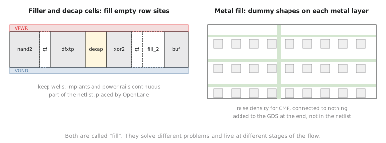
A quick way to confirm the rows are complete is OpenROAD’s check_placement on the final DEF, which reports any overlaps or illegal placements, and to open the layout in KLayout and look for gaps in the n-well along the rows. There should be none.
Step two: metal density
Now the routing layers. Run the density checks from the PDK’s KLayout deck on the final GDS. Which deck file holds them depends on the PDK version, as you found in the previous article; the general form of a batch KLayout run is:
klayout -b -r <density deck from the previous article> \
        -rd input=runs/uart_full/results/final/gds/uart_top.gds \
        -rd report=uart_density.xml
For the UART, the summary looks like this (simplified):
Layer   Windows   Below minimum   Above maximum
li1       342          0               0
met1      342          0               0
met2      342          6               0
met3      342         31               0
met4      342         88               0
met5      342        120               0
This pattern is typical for a small digital block. The lower layers are dense with cell internals, rails and local routing, so they pass. met3 and above carry a few long signal routes and the power straps, with a lot of empty space in between, so many windows fall below the minimum. Nothing is anywhere near the maximum.
These are the windows metal fill exists for. On an open shuttle, the provider’s tapeout scripts generate metal fill across the whole chip, including your block, and check density on the result. If you are preparing a block for such a shuttle, the useful thing to check yourself is that nothing in your layout blocks fill from being placed where it is needed, and that no window is above the maximum, since fill cannot fix that. If you are responsible for the whole chip, you run the fill generator yourself and then re-run this check until every window passes.
Checking that fill broke nothing
Fill adds real geometry, and real geometry is subject to the same rules as everything else. Re-run the DRC script from Section 8.1 on the final GDS, the one with filler and decap cells and, if you generated it, metal fill:
COUNT: 0
Then LVS again, extracting from the final GDS and comparing with the final netlist as in Section 8.2:
Final result: Circuits match uniquely.
The filler and decap cells are in both the layout and the final netlist, so they match like any other cell. Metal fill shapes are not connected to anything, so extraction sees them as isolated pieces of metal with no devices, and the LVS setup ignores them. If your LVS run ever reports thousands of extra nets or devices after fill, check that the setup and the extraction treat dummy fill correctly before assuming the fill itself did something wrong.
What the design has now passed
The UART that came into this module was placed, clocked, routed and timing clean, and nothing more had been checked. It leaves the module having passed every independent geometric, electrical and manufacturability check a signoff needs:
| Check | Section | Status |
|---|---|---|
| Design rule checking | 8.1 | Clean: the layout can be manufactured |
| Layout vs. schematic | 8.2 | Clean: the layout implements the final netlist |
| Antenna rules | 8.3 | Clean: no gate oxide at risk during fabrication |
| IR drop | 8.4 | Verified: supply drop far below the budget everywhere |
| Electromigration | 8.4 | Verified: grid currents within limits |
| Fill and density | 8.5 | Rows complete; density checked, with metal fill needed on the upper layers at tapeout |
Notice that timing is not on this list. A design can be timing clean and still fail every row of that table, and the other way round. Physical verification is independent of timing closure. A tapeout decision needs both, and neither replaces the other.
Practice Exercise
Without looking back at the table, name for each of the six checks one thing a design could get wrong that only that check would catch.
Solution
- DRC: a shape too narrow, or too close to another, to be reliably printed and etched. A purely geometric problem no other check looks at.
- LVS: two nets shorted, or one net broken open, by a layout defect that is perfectly legal geometry. DRC cannot see connectivity.
- Antenna rules: a net whose metal, at one etch step, collects enough charge to damage the gate it is connected to, during fabrication, before the chip even exists.
- IR drop: a cell that is correctly connected and geometrically fine, but gets a supply too far below nominal because of resistive loss in the grid under real current.
- Electromigration: a grid wire that is fine on day one and passes every other check, but carries enough steady current density to wear through over years of use.
- Fill and density: a layout that is correct in every functional and electrical sense, but with metal density so uneven that CMP cannot planarise it reliably. The only check here that is not about the design’s function at all.
With a design that has passed DRC, LVS, antenna, IR drop, electromigration and density checks, Module 9 turns the verified layout into the file a fab actually receives: GDSII streaming, an independent review in KLayout, and a signoff checklist that brings together everything from Modules 7 and 8 into one final go or no-go decision.