Closing the Loop on Module 3's Power Grid
In Module 3 we designed the UART’s power grid before any cell had a real location: rings, straps, and a rough idea of IR drop from an estimated current and an assumed grid resistance. It had to be a guess, because there was nothing yet to measure. Now the UART is placed, clocked, routed, and clean for DRC, LVS and antenna rules. In this section we check whether the grid actually does its job.
The intuition, recalled
The relationship is the same as in Module 3, Ohm’s law applied to a resistive grid instead of a single resistor:
$$ V_{drop} = I \times R $$
Every cell draws current from the grid, mostly when it switches. That current travels from where power enters the design, through the rings and straps, down into the cell rows’ rails, and every piece of metal on the way has resistance. So every segment drops a little voltage, and a cell far from the supply, fed through a long, thin path, sees a lower supply than a cell right next to it.
Figure 1 shows the simplest case, one strap fed from one end. The current in each segment is the sum of everything drawn downstream of it, so the segments nearest the supply carry the most current and the drop builds up along the strap.
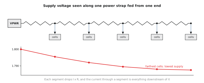
IR drop is not a defect as such. It is a margin that has to be budgeted and checked, in the same way as setup and hold margins. A lower supply makes cells slower, so a big drop in one region can turn a path that met timing at the library’s nominal voltage into one that fails.
What has changed since the estimate
The Module 3 estimate rested on three assumptions, and each can now be replaced by real data:
- Current. We now have the real, timing-closed netlist, so OpenSTA can compute each cell’s power from its Liberty data, its real load and a switching activity. The activity is either a default assumption (vectorless) or, better, taken from a simulation of the design doing real work.
- Grid geometry. The rings and straps OpenLane’s PDN generator actually built, including any local changes made during placement and routing.
- Resistance. The real sheet resistance of each SKY130 metal layer applied to the real lengths and widths, plus the resistance of every via stack between layers.
| Module 3 (planning) | Module 8 (verification) | |
|---|---|---|
| Current | Estimated from typical activity | Computed per cell from the real netlist and an activity source |
| Grid geometry | Planned strap spacing and width | The grid actually built |
| Purpose | Size the grid so it will probably be fine | Confirm it is fine, or find where it is not |
This is the same pattern as timing: an early estimate lets you make a sensible decision before the data exists, and a late check confirms it once the data does.
A worked segment
Take one segment of a met4 strap, 200 µm long and 4 µm wide. SKY130’s met4 has a sheet resistance of roughly 47 mΩ per square (check the PDK for the exact figure). The number of squares along the strap is
$$ N_{squares} = \frac{\text{length}}{\text{width}} = \frac{200\ \mu m}{4\ \mu m} = 50 $$
so its resistance is
$$ R = 50 \times 0.047\ \Omega \approx 2.35\ \Omega $$
In a larger design, the cells fed through this segment might draw 8 mA at a moment of heavy switching. The drop across this one segment is then
$$ V_{drop} = 0.008\ A \times 2.35\ \Omega \approx 19\ mV $$
A common budget is around 5% of the supply, 90 mV on a 1.8 V rail, so 19 mV on one segment is fine on its own. But a far cell is fed through many segments in series, plus rails and vias, and it is the total along that path that counts. For our small UART the currents are far lower than 8 mA, as we will see in the lab, but the arithmetic is the same.
The mistake to avoid is computing one segment and calling it done. A cell’s supply is set by the drop along the whole path from the supply to that cell. The worst cell in a design is rarely next to the single worst segment. It is at the end of the longest, most heavily loaded resistive path, and finding it needs a tool that solves the whole grid at once.
Hands-on: find the real sheet resistance
Do not take my 47 mΩ on trust. Magic’s technology file lists the sheet resistance it uses for extraction, in milliohms per square:
grep -n "^ *resist " "$PDK_ROOT/sky130A/libs.tech/magic/sky130A.tech" | head -20
The values differ a lot between layers. li1 is around 12.8 Ω per square, met1 and met2 around 0.125 Ω, met3 and met4 around 0.047 Ω and met5 lower still. This is why power grids are built on the thick upper metals and not on met1, and why the standard cell rails, which are met1, are kept short between strap connections.
Practice Exercise
A strap segment on met5 is 150 µm long and 6 µm wide, with a sheet resistance of about 0.0285 Ω per square, and carries 12 mA. What is the drop across this segment, and would it be a concern on its own against a 90 mV budget?
Solution
Squares: 150 / 6 = 25.
Resistance: 25 × 0.0285 ≈ 0.71 Ω.
Drop: 0.012 A × 0.71 Ω ≈ 8.6 mV.
On its own this segment is well within the budget, and as the text says, a single segment rarely is the problem. What matters is its share of the total drop along the path to the farthest cell it helps supply, which is what the IR drop tool in the lab computes.
IR drop is about voltage now. In the next article we look at a related but different concern that shows up over the chip’s lifetime: electromigration, and why every piece of metal has a current density limit.