Diagnosing a Real LVS Mismatch
In the previous article we saw a clean LVS report. A failing one is more interesting, because Netgen does not only say “these do not match”. In its own vocabulary it tells you roughly what kind of mismatch it found. Learning to read that vocabulary is the real skill here; running the tool is the easy part. In this article we break the UART on purpose and read the result.
Introducing a deliberate error
Take the layout from the previous article and remove one via: the met1 to met2 via that connects the baud-rate divider’s output net, baud_div_out, to the enable (GATE) pin of the transmit clock gate, a sky130_fd_sc_hd__dlclkp_1 cell. In Magic:
load uart_top
box 76.400um 48.220um 76.460um 48.280um
select area via1
what
delete
save uart_top_broken
gds write uart_top_broken.gds
Deleting the via removes no metal. The met1 and met2 segments are both still there and still pass every spacing rule. They were never meant to be spaced apart; they were meant to be connected. This is a pure connectivity defect, an open circuit that DRC cannot see. It is the blind spot from two articles ago in the other direction: a connection that should exist and does not, instead of one that should not exist and does.
Running LVS again
Extract from the broken layout and run the same Netgen comparison:
magic -dnull -noconsole \
      -rcfile "$PDK_ROOT/sky130A/libs.tech/magic/sky130A.magicrc" <<'EOF'
gds read uart_top_broken.gds
load uart_top_broken
select top cell
extract do local
extract all
ext2spice lvs
ext2spice -o uart_broken_extracted.spice
quit -noprompt
EOF

netgen -batch lvs \
  "uart_broken_extracted.spice uart_top_broken" \
  "runs/uart_full/results/final/verilog/gl/uart_top.v uart_top" \
  "$PDK_ROOT/sky130A/libs.tech/netgen/sky130A_setup.tcl" \
  uart_lvs_broken.report
The report is long when things fail. The parts that matter, trimmed and simplified a little, are:
Number of devices: 1406                     |Number of devices: 1406
Number of nets: 1843 **Mismatch**           |Number of nets: 1842 **Mismatch**

...
Net: baud_div_out                           |Net: baud_div_out
  sky130_fd_sc_hd__dfxtp_2/Q = 1            |  sky130_fd_sc_hd__dfxtp_2/Q = 1
  sky130_fd_sc_hd__and2_1/A = 2             |  sky130_fd_sc_hd__and2_1/A = 2
  sky130_fd_sc_hd__nor2_1/B = 1             |  sky130_fd_sc_hd__nor2_1/B = 1
                                            |  sky130_fd_sc_hd__dlclkp_1/GATE = 1
Net: a_76400_48220#                         |(no matching net)
  sky130_fd_sc_hd__dlclkp_1/GATE = 1        |
...
Netlists do not match.
Reading the signature
Three kinds of defect, an open, a short and a wrong device, each leave a different fingerprint in the report, and you can usually tell them apart from the numbers alone, without opening the layout.
| Signature | What you see in the report | What it means |
|---|---|---|
| Open | The layout has more nets than the netlist. One netlist net matches a layout net that is missing some pins, and a new, unmatched layout net holds the rest | A connection that should exist does not. The metal on either side of a missing via or contact forms two separate nodes |
| Short | The layout has fewer nets. One layout net carries the combined pins of two netlist nets | Two shapes touching or merging made one node out of two, the scenario from two articles ago |
| Device mismatch | Net counts can match, but a cell count differs, or an instance has different pins or connections | The wrong cell is in the layout: a substituted cell, or a library or extraction mapping problem, not a routing defect |
Look at our report against the table. The layout has one more net than the netlist, 1843 against 1842. The netlist’s baud_div_out has five pins; its layout counterpart has only four, and the fifth, the GATE pin of the clock gate, sits alone on a new net that Magic had to invent a name for from its coordinates (a_76400_48220#). That is the textbook open. Figure 1 shows how to get from the report to the kind of defect.
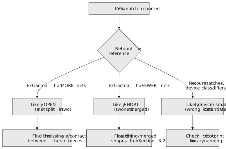
The pin lists are your map. baud_div_out split into a piece with the clock gate’s GATE pin and a piece with everything else. That tells you exactly which connection broke, the one between those two pieces, without opening the layout. In a design with thousands of nets that is the difference between a two-minute diagnosis and hours of searching. The auto-generated name even gives you coordinates to start from.
A common mistake is to see “Netlists do not match” and assume the reference netlist is wrong. In this flow the final netlist is the reference by construction, and LVS exists to check that the layout still implements it. Start from the assumption that the physical implementation introduced the defect, unless you have a specific reason to think the netlist changed, for example a manual layout edit whose matching netlist edit was never made.
Confirming the fix
Put the via back, extract again and compare again. The loop is the same as the DRC fix cycle in Section 8.1, only with the LVS report:
load uart_top_broken
box 76.400um 48.220um 76.460um 48.280um
paint via1
save uart_top_fixed
gds write uart_top_fixed.gds
Then the same extract-and-compare sequence. A correct fix joins the two pieces of baud_div_out back into one five-pin net, the net counts become equal again and the report ends with Circuits match uniquely.
Practice Exercise
A Netgen report shows the layout has one fewer net than the netlist. In the detail, a single layout net lists the pins of both rx_bit and rx_parity_ok from the netlist. Using the table above, is this an open, a short or a device mismatch, and what would you look for in the layout?
Solution
This is a short. The layout has fewer nets than the netlist, and two nets that should be separate, rx_bit and rx_parity_ok, appear as one node in the layout.
Look for geometry of those two nets that touches or overlaps: most likely two routed segments on the same layer that were joined by a jog or a manual edit, as in Figure 1 of the first article in this section, or a via placed so that it bridges both nets at once. Separate the geometry, with the same nudge-or-reroute reasoning as the DRC fixes, then run DRC as well as LVS, because separating the shapes creates a new gap that has to meet the spacing rules.
DRC and LVS both check the finished layout as a static object. In the next section we look at a defect that is neither geometric nor about connectivity: the antenna effect, which damages the chip while it is still being manufactured.