What DRC Actually Checks, and Why Every Rule Exists
In the previous module we signed off the UART’s timing. In this module we check the layout itself, and the first check is Design Rule Checking. Nobody at the fab looks at your GDS and decides it looks buildable. Before the layout gets anywhere near a wafer it has to pass an automated check of every shape on every layer against a few thousand geometric rules, and a single shape a few nanometres too close to its neighbour is enough to stop it.
It is tempting to see DRC as paperwork. I find it more useful to read each rule as a statement about what a piece of fabrication equipment can or cannot reliably do. Read that way, a DRC violation stops being a mysterious complaint and becomes useful information about why the layout cannot be built as drawn.
A rule is a manufacturing limit with a number on it
Think about what happens to your GDS after it leaves your hands. Each layer becomes a photomask. Light is projected through the mask onto a wafer coated in resist, the exposed resist is developed, and the pattern is etched into the material below: polysilicon, metal or oxide. This is repeated layer after layer, each one aligned to the layers before it.
Every one of those steps has limits. Light diffracts, etch chemistry does not stop exactly at the drawn edge, and one mask never lines up perfectly with the previous one. DRC rules are those limits written down as “shapes must be at least this wide” and “shapes must be at least this far apart”.
| Rule category | What it checks | The manufacturing limit behind it |
|---|---|---|
| Minimum width | A shape cannot be narrower than X | Below a certain width lithography cannot resolve the shape reliably. It may not print at all, or print with edges too rough to be electrically predictable |
| Minimum spacing | Two shapes on the same layer cannot be closer than X | Diffraction and etch bias blur edges, so shapes drawn too close can bridge into one during etch even though the mask shows them apart |
| Enclosure | Shape A must extend past shape B by at least X | Mask-to-mask alignment is never perfect; the margin makes sure a via still lands fully inside its metal if the layers shift slightly |
| Minimum area | A shape cannot be smaller than X in area | Very small shapes can lift off or disappear during processing, and their properties become unpredictable |
| Notch and extension | Extra rules for inside corners and stubs | Sharp inside corners and dead-end stubs are where lithography rounding distorts a shape most |
None of these exists “because the rulebook says so”. Each one is a margin against a specific, repeatable source of error in the fab. A spacing rule is not protecting you from your own mistake. It protects against the fact that two features that are clearly separate on your screen may not stay separate once diffraction and etch have had their say. Figure 1 shows three of the categories.
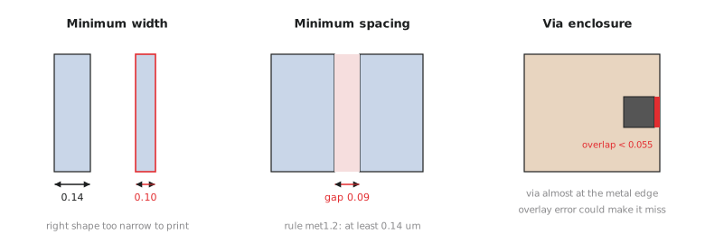
A DRC deck is really a compressed description of one fab’s process capability. Two foundries offering a “130 nm” process can have noticeably different decks, because their lithography and etch tools have different limits. The rules are not universal physics. They belong to that fab’s equipment.
Worked example: spot the violation by hand
SKY130’s rule for spacing between two met1 shapes, rule met1.2 in the PDK documentation, is 0.14 µm. Let us check two routed segments against it.
Segment A occupies x = 10.000 to 10.230 µm. Segment B occupies x = 10.320 to 10.500 µm, on the same layer and over the same y range, so they really are side by side.
$$ \text{gap} = 10.320 - 10.230 = 0.090\ \mu m $$
$$ 0.090\ \mu m < 0.14\ \mu m \implies \text{violation} $$
That is the whole mechanism a DRC engine runs, millions of times, across every pair of shapes on every layer. It does not understand your circuit, your clocks or your netlist. It is a geometric checker working at enormous scale.
One mistake I see is assuming spacing rules only apply between shapes on different nets. DRC has no concept of a net at all. Two pieces of the same net routed too close around a tight corner can trip exactly the same rule as two unrelated nets. Geometry does not know what it is connected to. Connectivity is LVS’s job, which is the subject of the next section.
Hands-on: find a real SKY130 rule in the PDK
Do not take numbers from a course on trust. Go and find them. With the PDK installed (Module 1), the rules are in the tool decks under the PDK root:
# The Magic tech file, which Magic's DRC reads
grep -n "met1.2\|li.3" "$PDK_ROOT/sky130A/libs.tech/magic/sky130A.tech" | head

# The KLayout rule deck, a second, independent implementation
ls "$PDK_ROOT/sky130A/libs.tech/klayout/drc/"
SKY130’s rules follow a layer.number naming scheme, such as met1.2 or li.3, and the same names appear in the PDK’s design rule documentation with a short explanation of each. The number you want to remember is not the value itself but how to find it, because that is what Magic will check the UART against in the next article.
Practice Exercise
SKY130’s rule for spacing between two via cuts (the cut between met1 and met2) is 0.17 µm, measured edge to edge. Via A spans x = 20.00 to 20.15 µm. Via B spans x = 20.29 to 20.44 µm, over the same y range. Is this pair compliant?
Solution
Gap = 20.29 − 20.15 = 0.14 µm.
0.14 µm < 0.17 µm, so this is a violation. The vias are 0.03 µm too close.
A routed design contains this check thousands of times over, which is why it is automated, but the arithmetic never gets harder than this.
In the next article we stop working by hand and run Magic’s DRC engine on the routed UART against the real SKY130 rule deck.