What Is an Antenna Diode and Why Do We Need It?
What Is an Antenna Diode?
An antenna diode is a protection diode placed in a digital integrated circuit to guard transistor gates against damage during the chip fabrication process. It has nothing to do with radio antennas. The name comes from the “antenna effect,” a phenomenon that occurs during plasma etching. Formally, this failure mode is called Plasma Induced Gate Oxide Damage — “antenna effect” is just the shorthand VLSI engineers use day to day.
The Antenna Effect
Modern ICs are built layer by layer. Metal interconnects and polysilicon wires are patterned using plasma etching, a process where ionized gas (plasma) selectively removes material. During this process, conductive structures like metal wires and polysilicon lines collect charge from the plasma.
Here’s the timing detail that makes this dangerous: while a given metal (or polysilicon) layer is being etched, each net’s conductor is briefly isolated — it’s already wired to a transistor gate, but it hasn’t yet been connected down through a via/contact to a source/drain junction or substrate. In that window, it is electrically “floating” except for its connection to the gate, so any charge the plasma deposits on it has nowhere to go but into the gate oxide. This isolation-then-charge-collection repeats at every metal layer a net passes through until it’s finally tied down.
Because a MOSFET gate is isolated by a thin oxide layer (just a few nanometers thick), there is nowhere for this charge to go. As the antenna’s potential rises, the electric field across the oxide rises with it, until it’s strong enough to drive Fowler-Nordheim tunneling — electrons tunneling directly through the thin oxide’s potential barrier. Depending on how much charge accumulates, this either ruptures the oxide immediately or, at lower levels, accumulates as time-dependent dielectric breakdown (TDDB) — cumulative wear that shows up later as a reliability failure rather than an instant, visible defect.
This charge accumulation on a floating conductor is the antenna effect. The “antenna” is the long wire or metal polygon acting like a receiving antenna, collecting charge.
Antenna Ratio
The severity of the antenna effect is measured by the antenna ratio:
Antenna Ratio = Area of metal connected to gate / Area of the gate oxide
Design rules specify a maximum allowable antenna ratio (commonly 400:1 to 1000:1 depending on the process). Violating this rule increases the risk of gate oxide damage.
This ratio is checked separately at every interconnect layer during antenna rule checking (ARC) — a net that’s clean at metal 1 can still violate the rule once it’s extended up to metal 3. Foundry ARC flows typically run three related checks per layer: a metal area rule (conductor area vs. gate area), a perimeter rule (conductor perimeter × thickness vs. gate area), and a via/contact area rule. A violation on any one of the three flags the net for a fix.
How Does an Antenna Diode Help?
An antenna diode provides a discharge path for the accumulated charge before it can damage the gate oxide.
The diode is placed between the offending net and a supply rail (typically VDD or VSS):
- A reverse-biased diode to VSS bleeds excess positive charge to ground.
- A reverse-biased diode to VDD bleeds excess negative charge to the supply.
During normal circuit operation (after fabrication), the diode remains reverse biased and has no effect on circuit behavior — it is essentially invisible to the design. Its only job is to protect the gate during manufacturing.
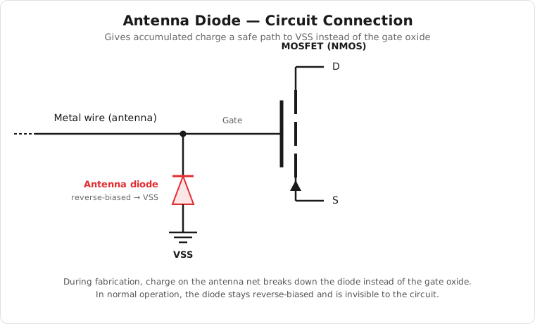
Why this works: a p-n junction breaks down (or turns on) at a lower voltage than the gate oxide can withstand. Wiring the net to that junction makes the diode the “weakest link” — it fails safely and non-destructively, well before the oxide ever sees a damaging field. This is also why tying a net to any active-area junction, not just a dedicated diode, relaxes its antenna ratio calculation: the moment there’s a path to substrate, the isolated-antenna condition disappears.
A caveat for advanced nodes: as gate oxides get thinner (16 nm and below), the voltage margin between “diode breaks down” and “oxide breaks down” shrinks. The classic guarantee that the diode always wins is most reliable in older, thicker-oxide processes — in advanced nodes, jumpering (see below) becomes relatively more important as a primary defense rather than just a cleanup technique.
Where Are Antenna Diodes Inserted?
Antenna diodes are added in two ways:
- Manually by the designer — when a known long net violates the antenna rule.
- Automatically by EDA tools — place-and-route tools (like OpenLane/OpenROAD) run an antenna rule check (ARC) after routing and insert diodes automatically on violating nets.
In OpenLane, the antenna check is performed by the OpenROAD antenna_check command, and diode insertion is handled during detailed routing or as a post-route fix step.
Why Not Just Fix the Routing?
Sometimes the antenna violation can be resolved by metal jumpers — routing the wire up to a higher metal layer and back down. This defers the net’s final connection to the gate, so it spends less time exposed as a floating antenna during etching, reducing charge buildup. However, jumpering consumes routing resources and isn’t always feasible.
In practice, EDA flows often prefer jumpers where routing allows — they add no extra junction capacitance to the net — and fall back to diode insertion to clean up whatever violations remain. Antenna diodes are cheap in area and simple to insert automatically, but each one adds a small amount of junction capacitance to the net it protects.
Summary
| Aspect | Detail |
|---|---|
| Problem | Charge buildup on floating conductors during plasma etching damages gate oxide |
| Solution | Antenna diode provides a discharge path to VSS or VDD |
| Active during | Fabrication only (reverse biased in normal operation) |
| Inserted by | Designer manually, or EDA tool automatically |
| Cost | Small area overhead, no performance impact |
Antenna diodes are a small but essential element of robust IC design. Without them, long interconnects in deep-submicron processes would regularly destroy the very transistors they are meant to connect.