From Schematics to Code
In 1971 Intel shipped the 4004, the first microprocessor on a single chip: 2300 transistors, 740 kHz, about 12 mm² of silicon, designed almost entirely by hand. Transistors were placed on paper, wires routed by eye, and the masks were cut from rubylith on light tables. It took a small team about a year.
A top-end processor today has over a hundred billion transistors and takes a team of thousands two or three years. Those thousands are not cutting rubylith. They are writing text. This article is about what changed in between, and it is the reason Verilog exists.
The wall
Hand design worked up to something like ten thousand transistors. At that size one careful engineer could hold a printed schematic in their head, check every connection, and find mistakes by looking. Through the late 1970s and 1980s density doubled every eighteen months or so, and by the mid-1980s chips had a million transistors. A million-transistor schematic at a transistor per square centimetre is bigger than a football pitch. Nobody checks that by eye. The workflow of draw, route, inspect had not merely become slow; it had become impossible.
What changed was the level at which the engineer worked.
Describe behaviour, synthesise structure
The idea behind all electronic design automation is short: if you can write down precisely what a circuit should do, a program can work out how to build it. Instead of drawing every gate, the engineer writes “take two 8-bit numbers and produce their 9-bit sum”, and a synthesis tool chooses the gates, connects them, and optimises for speed or area. The engineer thinks about what; the tool handles how.
The value is not that you write less. For a small circuit a Verilog description is often longer than the schematic. The value is that everything downstream, implementation and verification, becomes automatic, and that is what lets a few thousand people design something with a hundred billion parts. It is the same move as going from assembly language to a compiled language: you give up control of every detail for the ability to say what you mean and let a tool translate it.
Where Verilog came from
Verilog was not an academic project or a standards effort. It was built by a small company to sell a simulator.
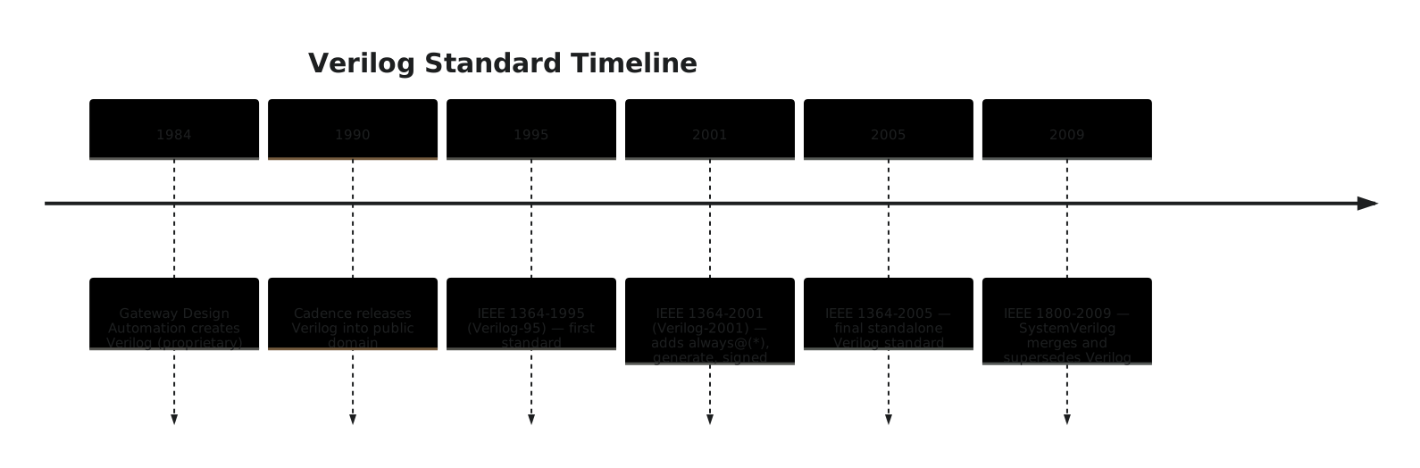
In 1984 Phil Moorby and Prabhu Goel at Gateway Design Automation in Massachusetts created Verilog as the input language for their simulator. It was compact, looked enough like C that engineers took to it, and could describe any digital circuit. It spread through the US and Asian markets on the strength of the simulator.
Cadence bought Gateway in 1989 and in 1990 put the language into the public domain. That was business, not charity: Cadence sold tools, and an open language meant a bigger market for them. Open Verilog International took over the specification and other vendors built simulators and synthesisers around it.
In 1995 it became IEEE 1364-1995, Verilog-95, the first formal standard anyone could implement without a licence from Cadence: modules, ports, wire and reg, continuous assignment, procedural blocks and gate primitives.
The 2001 revision, IEEE 1364-2001, is the one that matters. It added always @(*), which removed a whole class of simulation and synthesis mismatches; ANSI-style port declarations; generate blocks; signed arithmetic; multi-dimensional arrays; and $clog2. This is the version this course uses, and every tool, commercial or open source, accepts it.
Verilog-2005 was a maintenance release and the last standalone Verilog. In 2005 the IEEE also published SystemVerilog, IEEE 1800, a superset that added classes, constrained random stimulus, assertions and a richer type system, and in 2009 the two standards were merged (Figure 1). SystemVerilog is the industry standard now. Its RTL subset is Verilog-2001 with conveniences, so everything here carries over.
What you get
Simulation before silicon. You can run a design through millions of test cases before any wafer is started. A bug found in simulation costs an afternoon. The same bug found after fabrication costs a re-spin, which for a modern process is well into seven figures and months of delay.
Synthesis. The tool turns your description into an optimised gate netlist for whatever target you name, a standard-cell library for an ASIC or lookup tables for an FPGA, and does the Boolean optimisation and technology mapping itself.
Reuse. Write an N-bit adder once, instantiate it at 4, 8 and 32 bits in the same design.
Portability. The same RTL goes to an FPGA for prototyping and to an ASIC for production.
Collaboration. Twenty engineers work on twenty modules, in version control, and integrate through agreed port lists. Try that with one enormous schematic.
The abstraction stack
A chip is designed at several levels at once (Figure 2). At the top is the algorithm. Below it is RTL, register transfer level, which says what is stored in registers and what logic sits between them; that is where the RTL engineer works and where this course lives. Below RTL are gates, then transistors, then layout, then the fabrication process, and each is handled by tools driven by constraints from the level above.
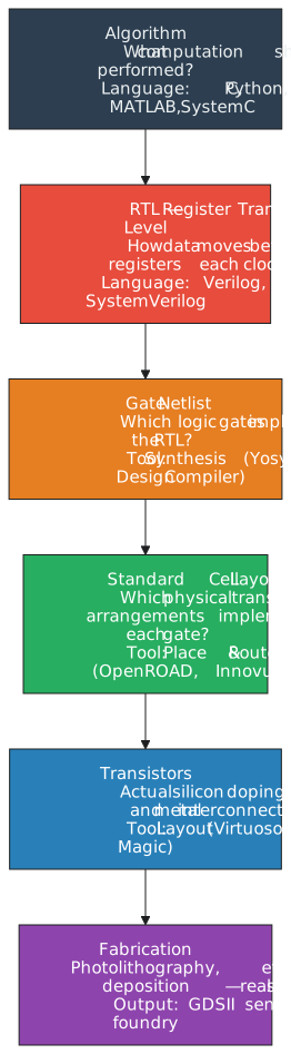
The algorithm engineer does not care which gates make the adder. The RTL engineer does not care which transistors make the NAND. The layout engineer does not care about the doping profile. Each layer hides a great deal from the one above it, and that hiding is what makes a billion-transistor design a human-sized job.
A sense of scale
A four-core desktop processor has on the order of ten billion transistors, a few hundred million flip-flops, and tens of millions of lines of RTL. If an engineer could verify a thousand connections a day, checking ten billion by hand would take tens of thousands of engineer-years. With an HDL and the tools around it, a team of a thousand does it in two or three years. That is not a productivity gain; it is the difference between possible and not.
Every chip you own was designed this way: described in Verilog or SystemVerilog, simulated, synthesised and sent to a foundry as a layout file. The next article is about the first thing that trips people up in that process: the same Verilog file is read by two different tools with two different sets of rules.