IR Drop, Intuitively
The previous article built a grid. This one is about why the grid has to be dense enough.
An uncomfortable fact about the wires carrying VDD to your cells: they are not perfect conductors. They have resistance like everything else on the chip, and whenever current flows through resistance, voltage is lost along the way. So a cell next to a strap and a cell far from every strap are not running at the same supply voltage. The far one runs at slightly less than VDD, and if it is less enough, that cell switches slower or, in the worst case, misbehaves. This is IR drop.
The relationship
It is Ohm’s law applied to a wire instead of a resistor on a schematic:
$$V_{\text{drop}} = I \times R$$
Current $I$ flows from the strap, along the metal, to a cell. The metal has resistance $R$, small but not zero. The product is voltage lost before it reaches the cell, which sees VDD minus that drop. Two things make it worse, and both map onto layout decisions you are already making:
- Longer distance from a strap means more metal, more resistance, more drop. That is why straps exist: shorten the distance and the drop shrinks.
- More current demand in one area means more current through the same resistive path, more drop for the same distance. That is why placement density and switching activity (which you will influence from Module 4 on) matter to power integrity too.
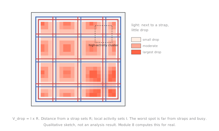
IR drop is why the grid is not only about getting current somewhere into the core. It is about getting it everywhere with roughly equal ease, to every cell regardless of where it sits. Uneven strap coverage gives uneven voltage across the die, a subtler and nastier bug than an open circuit, because the chip may still work, with degraded timing margin in exactly the spots you did not check.
Reasoning about it by hand
You do not need an IR drop tool for the intuition. That is Module 8’s job, once you have real extracted parasitics and a switching activity profile to feed it. Right now you can reason about relative risk from the floorplan sketch alone.
Take the counter8 core with its ring and strap grid, and suppose, for the exercise, that the switching current is concentrated near the counter’s increment logic and that this cluster sits in one corner. Figure 1 shades the result. Which region is under the most risk?
- A cell on a strap crossing, even next to the busy cluster, is the safest spot: minimal distance, minimal resistance, whatever the local current.
- A cell between straps, far from any crossing, is at moderate risk even under uniform current, because it is at the point of maximum distance from every strap.
- The busy cluster itself, if it also sits far from a strap, is worst on both counts: the most resistance and the most current through it.
This is why real PDN design is not “add a ring and call it done”. Designers deliberately route extra straps toward known high-activity regions (clock buffers, wide datapath muxes, anything switching every cycle) rather than spacing the grid uniformly. You are seeing the reasoning now; Module 8 gives you the tool to confirm it.
Practice Exercise
A core has straps every 20 µm, and one standard cell row sits 18 µm from the nearest strap, near the worst case for that grid. A design change moves a high-fanout clock buffer into that row, roughly tripling the local current. Qualitatively, what happens to the row’s IR drop risk, and what is the most direct floorplan-level fix?
Solution
Risk rises sharply. The row was already near worst-case distance from a strap, and with $V_{\text{drop}} = I \times R$, tripling $I$ roughly triples the drop for the same path. The most direct floorplan-level fix is to add or move a strap closer to that row, shortening $R$ to compensate for the higher $I$. This is a floorplanning and PDN decision, not something synthesis or RTL should be asked to solve.
You now have the intuition. In the next article we look at the OpenLane config knobs that turn a ring-and-strap sketch into a real, tool-generated power grid.