Power Rings and Straps
Section 3.1 gave counter8 a die and a core. Section 3.2 is about getting power to what will be placed inside it.
Every standard cell in counter8 has a VPWR pin and a VGND pin next to its logic pins, and each one needs to reach a supply rail reliably, with low resistance, every clock cycle, for the life of the chip. Nothing in synthesis said how. It is a purely physical concern, and the first thing you design after the floorplan’s shape. The answer is a grid, and it is worth understanding why a grid specifically.
Why not one wide wire?
The naive idea: run one thick wire around the core carrying VDD, another carrying GND, and let every cell tap the nearest. That is the first piece of the real answer. It is called a power ring, and every OpenLane floorplan has one. But a ring alone leaves the interior starved. Cells near the edge are close to the ring; cells in the middle of a large core are far from it, and every micron of metal between a cell and its supply adds resistance, which adds voltage drop under load (the next article).
The fix is to also run wires across the interior, power straps, connected back to the ring, so no cell is more than a short hop from a low-resistance path to VDD or GND.
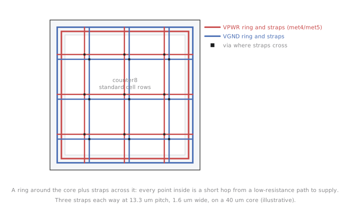
Together the ring and straps form the power distribution network, the PDN. It is a grid, a mesh of VDD and VGND wires, because a grid gives every point in the core several short paths to supply rather than one long path from one source. A city’s water system is not one pipe from the reservoir to every house for the same reason.
Reading the sketch
Figure 1 is the floorplan this module built, a 40 by 40 µm core in a 50 by 50 µm die, with a ring around the core and three vertical and three horizontal straps across the interior. Every standard cell row crosses at least one horizontal strap, the interior is bounded by the vertical straps, and the whole thing ties back to the ring at the edges. Where a horizontal strap crosses a vertical one of the same net, a via joins them, which is what makes it a mesh rather than two independent sets of parallel wires. Count the crossings: three straps each way give nine per net.
On a real design this small the grid would probably be lighter; on a large one it would be far denser. The sketch is deliberately small enough to read. The third article in this section has OpenLane generate a real grid from a few config values.
Rings and straps are not drawn on arbitrary layers. They go on the thick, low-resistance upper metals, in SKY130 typically met4 and met5, because those carry current with less loss than the thin lower layers used for signal routing near the transistors. Module 6 comes back to this when it covers special-net routing.
Practice Exercise
A core is 100 µm wide and needs vertical straps no farther than 25 µm apart so every cell is close to a low-resistance path. Ignoring the ring, how many interior vertical straps does it need, evenly spaced?
Solution
Straps every 25 µm across 100 µm means straps at roughly 25, 50 and 75 µm, three interior straps, which with the ring’s own edges at 0 and 100 µm gives four gaps of 25 µm. The general rule: interior straps = (width / spacing) − 1, here (100 / 25) − 1 = 3.
A ring and straps get current into the core. In the next article we ask the harder question: what happens to that current on its way to a cell far from any strap, and why does the answer matter well before Module 8 verifies it for real?