Project 4, Part 1: What an SRAM Datasheet Demands
Every previous project had a non-trivial datapath: a processor’s ALU and register file, a UART’s shift registers, an SPI master’s full-duplex logic. This one is different. The memory, from Section 3.6, is about as simple as a component gets. The whole challenge is timing discipline: reading a memory’s datasheet timing and translating it, exactly, into how many clock cycles the controller waits before trusting the memory’s response.
A realistic SRAM timing diagram
Real asynchronous SRAM chips, still common in embedded systems alongside synchronous alternatives, specify their behaviour with timing diagrams like Figure 1.
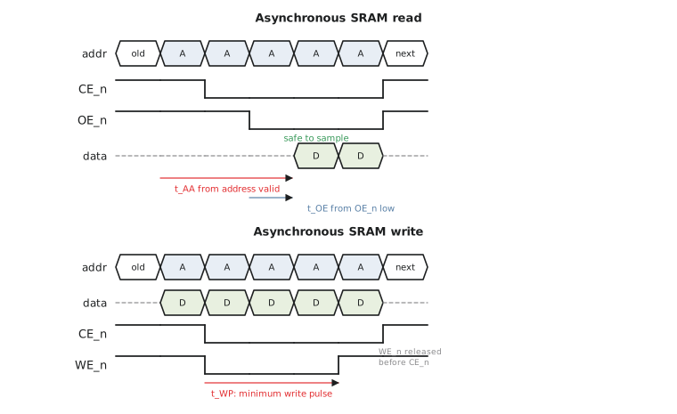
Two parameters matter most for a read: t_AA, address access time, how long after the address becomes valid before the data output is guaranteed correct; and t_OE, output enable time, how long after OE_n (active-low output enable) asserts before the data bus is driven. A controller has to wait for both before sampling the data bus. Reading too early samples garbage, not because anything is broken but because the memory has not finished responding.
Translating nanoseconds into clock cycles
Here is the calculation every memory controller design does, connecting back to the Section 8.3 timing discipline: given a system clock period, how many whole cycles satisfy a nanosecond requirement?
$$\text{Wait Cycles} = \left\lceil \frac{t_{AA}}{T_{clk}} \right\rceil$$
For $t_{AA} = 15$ ns and a 100 MHz controller ($T_{clk} = 10$ ns): $\lceil 15/10 \rceil = 2$ wait cycles. The controller holds the address stable and waits 2 full cycles before trusting the data bus, even though 15 ns is only 1.5 periods, because a synchronous design can only wait a whole number of cycles and rounding down would violate the datasheet. That is the same ceiling reasoning as the Section 8.3 critical-path calculation, applied to an external component’s datasheet instead of an internal gate delay. Never round a timing requirement down.
The read and write protocols
Read:
- Drive the address onto the address bus.
- Assert
CE_n(chip enable) andOE_n, both active-low. - Wait the calculated number of cycles (2 in the example) for
t_AAandt_OE. - Sample the data bus, now guaranteed valid.
- Deassert
CE_nandOE_n.
Write:
- Drive the address.
- Drive the write data onto the data bus.
- Assert
CE_nandWE_n(active-low write enable) together. - Hold for the datasheet’s write pulse width,
t_WP, using the same ceiling calculation. - Deassert
WE_nbefore deassertingCE_n. This ordering matters: releasing chip enable before write enable can leave the write pulse ill-defined from the memory’s point of view.
Why a parameterized behavioural model, not a real chip
This project verifies the controller against the parameterized memory model from Section 7.1, with one important addition: the model is extended to enforce timing, returning x if read too early, rather than the idealised always-correct memory used elsewhere. That is a deliberate testing technique worth naming: a timing-accurate behavioural model that fails loudly when a controller violates its contract is far more useful than a perfect memory that returns correct data even to a controller with a real timing bug. Real datasheets specify dozens of parameters beyond these three (address setup, chip enable to output valid, output disable time), each with its own minimum, and real verification environments build exactly this kind of model to catch a controller that “happens to work” against an idealised model but would fail against silicon.
Practice Exercise
A datasheet specifies $t_{WP}$, the minimum write pulse width, as 25 ns. How many wait cycles does a controller clocked at 133 MHz need to hold its write pulse?
Solution
$T_{clk} = 1/133\text{ MHz} \approx 7.52$ ns. $\text{Wait Cycles} = \lceil 25 / 7.52 \rceil = \lceil 3.32 \rceil = 4$. Three cycles ($3 \times 7.52 = 22.56$ ns) would violate the 25 ns minimum, which is why the ceiling function rather than nearest-integer rounding is correct: rounding 3.32 gives 3, which is unsafe, while the ceiling gives 4 and guarantees the pulse is at least as long as required.
An SRAM controller’s challenge is not the datapath. It is translating a datasheet’s nanosecond parameters into whole controller cycles with the ceiling discipline from Section 8.3, never rounding down. The read and write protocols are short explicit sequences whose durations come from the datasheet, not from convenient round numbers. In the next article we build the address decoding and the FSM that implements the two protocols.