Project 1, Part 3: The Control Unit
The previous article ended with a list: every mux select, write enable and PC decision the datapath needs but does not drive. This article builds the FSM that drives all of them, for every one of the eight instructions, in the two-block style Section 5.6 recommended as the default.
The state machine: fetch, decode, execute
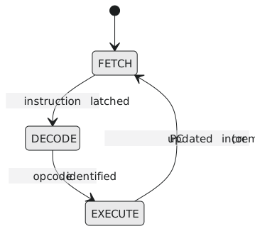
Three states, matching the first three steps of the cycle from the ISA article. The fourth step, advance, is folded into EXECUTE, since the PC update naturally happens as part of finishing an instruction rather than needing its own state.
The two-block implementation
typedef enum logic [1:0] {FETCH, DECODE, EXECUTE} cpu_state_t;
cpu_state_t state, next_state;

// Block 1: state register, exactly the Section 5.6 pattern
always_ff @(posedge clk or negedge rst_n) begin
    if (!rst_n) state <= FETCH;
    else        state <= next_state;
end

// Block 2: next-state logic AND all datapath control signals
always_comb begin
    // Safe defaults for every control signal: the Section 5.2 discipline,
    // now protecting a whole processor's worth of signals at once
    next_state    = state;
    reg_wr_en     = 1'b0;
    mem_we        = 1'b0;
    pc_write      = 1'b0;
    alu_b_sel     = 1'b0;
    wr_data_sel   = 2'b00;
    branch_taken  = 1'b0;

    unique case (state)
        FETCH: begin
            next_state = DECODE;
            // the instruction memory read is always active; nothing to drive here
        end

        DECODE: begin
            next_state = EXECUTE;
            // register file reads are combinational (Section 3.6 style):
            // rd_data_a and rd_data_b are valid as soon as Rd/Rs are decoded
        end

        EXECUTE: begin
            next_state = FETCH;
            unique case (opcode)
                3'b000, 3'b001, 3'b010, 3'b011: begin   // ADD, SUB, AND, OR
                    alu_b_sel   = 1'b0;    // select register Rs, not the immediate
                    reg_wr_en   = 1'b1;
                    wr_data_sel = 2'b00;   // write-back source: ALU result
                    pc_write    = 1'b1;    // advance PC normally
                end
                3'b100: begin   // LDI
                    reg_wr_en   = 1'b1;
                    wr_data_sel = 2'b10;   // write-back source: immediate
                    pc_write    = 1'b1;
                end
                3'b101: begin   // LD
                    reg_wr_en   = 1'b1;
                    wr_data_sel = 2'b01;   // write-back source: memory data
                    pc_write    = 1'b1;
                end
                3'b110: begin   // ST
                    mem_we      = 1'b1;
                    pc_write    = 1'b1;
                end
                3'b111: begin   // BEQ: branch if Rd is zero
                    branch_taken = (rd_data_a == 8'b0);
                    pc_write     = 1'b1;
                end
                default: ; // unreachable with a 3-bit opcode covering all 8 values,
                           // included anyway per the Section 5.6 safe-FSM discipline
            endcase
        end

        default: next_state = FETCH;   // safe-FSM recovery from any illegal state encoding
    endcase
end
Note the default assignments at the top of the combinational block. Every one of the seven control signals gets a safe do-nothing value before the case runs, the Section 5.2 latch-prevention discipline applied to a whole processor’s control in one block. Without it, any instruction whose EXECUTE branch forgot to set one signal would leave it latched at whatever the previous instruction left, a bug that only shows for particular instruction sequences, which is exactly the kind of subtle failure this discipline prevents.
Why three states, not one
Could fetch, decode and execute happen in one combinational pass, one clock per instruction? For this ISA and datapath, largely yes; nothing strictly requires three cycles. The project uses three deliberately, for a teaching reason: it makes each stage individually observable in a waveform (Section 6.5), which is worth far more for understanding what a processor does than a single-cycle version that computes the same result while hiding the structure the project exists to teach. A single-cycle version is a reasonable follow-on once the three-cycle version is verified.
Practice Exercise
Trace the control signals in EXECUTE for a BEQ where the tested register is not zero (branch not taken). Confirm the PC still advances.
Solution
With opcode = 3'b111 and rd_data_a != 0: branch_taken = 0, correctly not taken, but pc_write is still asserted unconditionally for this opcode. That matters. The control unit’s job on a not-taken branch is to fall through to the next sequential instruction like every other instruction, which requires the PC to advance (pc_write enables an update; branch_taken selects which value, the branch target or PC+1, is written). If pc_write were left deasserted on a not-taken branch, the processor would stop advancing and re-fetch the same BEQ forever, an easy bug to introduce and the reason for this exercise.
The control unit is a direct two-block FSM implementation of the cycle specified in the ISA article, with every mux select and write enable the datapath left undriven now assigned opcode by opcode inside EXECUTE. The Section 5.2 default-assignment discipline protects all of them from latch inference in one block, and the Section 5.6 default guarantees recovery from an unreachable encoding. In the next article, the last of this project, we assemble the datapath and control unit into one processor and prove it runs a real hand-assembled program.