Project 1, Part 1: The Instruction Set
The module introduction said every project starts with a specification. For a processor, that specification is the instruction set architecture (ISA): the complete contract between software (here, the hand-assembled test programs you will write) and the hardware you are about to build. Get this wrong and nothing downstream saves you, because every later stage of the project exists to satisfy what gets decided here.
Design goals
This is a deliberately minimal ISA, not because a real processor gets away with this little but because a small, complete instruction set teaches the structure of fetch, decode and execute more clearly than a large one, without changing how the pieces fit. The goals:
- 8-bit data width, matching the ALU from Modules 2 and 7.
- Enough instructions to write a real test program: arithmetic, conditional branching and memory access at minimum.
- A fixed, simple encoding: every instruction the same width, decoded the same way. That trades code density for decode simplicity, a defensible choice for a first processor.
The instruction set
| Mnemonic | Opcode (3 bits) | Format | Operation |
|---|---|---|---|
ADD Rd, Rs |
000 |
R-type | Rd <- Rd + Rs |
SUB Rd, Rs |
001 |
R-type | Rd <- Rd - Rs |
AND Rd, Rs |
010 |
R-type | Rd <- Rd & Rs |
OR Rd, Rs |
011 |
R-type | Rd <- Rd | Rs |
LDI Rd, Imm |
100 |
I-type | Rd <- Imm (immediate load) |
LD Rd, [Addr] |
101 |
I-type | Rd <- Mem[Addr] |
ST [Addr], Rd |
110 |
I-type | Mem[Addr] <- Rd |
BEQ Rd, Addr |
111 |
I-type | if (Rd == 0) PC <- Addr |
Eight opcodes exactly fill a 3-bit field, with no wasted encoding space and no need to steal a bit from elsewhere later. The set is minimal but complete: arithmetic (ADD, SUB), logic (AND, OR), an immediate load, memory access (LD, ST) and a conditional branch. That is everything a simple program needs to compute something, store it, and make a decision based on it. Note that BEQ tests a register against zero; that keeps the branch self-contained without needing a separate flags register.
Instruction encoding
Every instruction is 8 bits, matching the data width, so one instruction fetch is exactly one memory read:
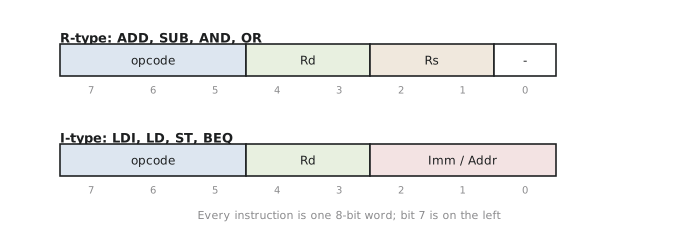
R-type (ADD, SUB, AND, OR):
  [7:5] opcode   [4:3] Rd (2-bit register select, 4 registers)   [2:1] Rs (2-bit)   [0] unused

I-type (LDI, LD, ST, BEQ):
  [7:5] opcode   [4:3] Rd   [2:0] Imm / Addr (3-bit)
The encoding forces an honest constraint. With 8 bits in total and 3 spent on the opcode, there is no room for a wide register select and a wide immediate in the same word. This project resolves it by keeping the register file at 4 entries (a 2-bit select) and giving the I-type instructions a 3-bit immediate or address. That is a real architectural trade-off, and one you should feel free to revisit as an extension once the base design works. A production ISA, even a simple one like RV32I, spends far more care on encoding efficiency; the point here is that you hit the width constraint yourself and make a decision about it rather than being handed a pre-solved encoding.
The fetch-decode-execute cycle as a specification
Before any RTL, state the cycle in plain words, precisely enough to be checkable later:
- Fetch: read the instruction at the address in the program counter (PC) from instruction memory.
- Decode: split the instruction into opcode, register selects and immediate/address, per the encoding above.
- Execute: perform the operation the opcode specifies: an ALU operation (Modules 2 and 7), a register file read or write (Module 3), a memory access (Module 7), or a conditional PC update.
- Advance: unless a taken branch has already updated the PC, increment it.
This four-step cycle is the specification the datapath (next article) and control unit (the one after) have to implement. Every register, mux and FSM state in the rest of the project exists to make these four steps happen, one instruction at a time.
Practice Exercise
Hand-assemble the following program into the 8-bit encoding: load 5 into R0, load 3 into R1, add R1 into R0, and store the result to memory address 0.
Solution
Using the I-type layout [opcode][Rd][Imm] for LDI and ST, and R-type [opcode][Rd][Rs][0] for ADD:
LDI R0, 5   ->  100 00 101     (opcode=100, Rd=00, Imm=101)
LDI R1, 3   ->  100 01 011     (opcode=100, Rd=01, Imm=011)
ADD R0, R1  ->  000 00 01 0    (opcode=000, Rd=00, Rs=01, bit 0 unused)
ST  [0], R0 ->  110 00 000     (opcode=110, Rd=00 is the source register, Addr=000)
This is what an assembler automates, and doing it by hand once is worth the tedium: it forces you to internalise the encoding you just designed in a way that jumping straight to writing an assembler (a natural follow-on project) would let you skip.
The ISA is the contract everything else has to satisfy: eight opcodes filling a 3-bit field, a fixed 8-bit word matching the data width, and a deliberately narrow register and immediate encoding that makes you feel the trade a wider ISA would resolve differently. In the next article we build the datapath, the registers, ALU and muxes that make these eight instructions executable.