Project 3, Part 2: The Shift Register and Chip Select
The previous article specified the modes. This one builds the datapath.
The structural difference between SPI and everything built for UART: SPI is full-duplex. Data moves in both directions, master to slave and slave to master, on every clock edge, at the same time. There is no separate transmit phase and receive phase. The shift register here is built around that simultaneity.
One register, two data lines
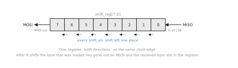
SPI uses two data lines, MOSI (master out, slave in) and MISO (master in, slave out), alongside the shared clock and an active-low chip select CS_n. The shift register’s job is to shift a bit out on MOSI at the same moment it shifts a new bit in from MISO, every clock edge, for as many bits as the transaction needs (8 here).
module spi_shift_reg #(parameter WIDTH = 8) (
    input  logic             clk, rst_n,
    input  logic             shift_en,        // one pulse per SPI bit period
    input  logic             load,            // load a new byte to transmit
    input  logic [WIDTH-1:0] tx_data,
    input  logic             miso,
    output logic             mosi,
    output logic [WIDTH-1:0] rx_data
);
    logic [WIDTH-1:0] shift_reg;

    assign mosi = shift_reg[WIDTH-1];   // MSB first, SPI's overwhelming convention

    always_ff @(posedge clk or negedge rst_n) begin
        if (!rst_n) begin
            shift_reg <= {WIDTH{1'b0}};
        end else if (load) begin
            shift_reg <= tx_data;
        end else if (shift_en) begin
            shift_reg <= {shift_reg[WIDTH-2:0], miso};   // shift LEFT, capturing miso at the bottom
        end
    end

    assign rx_data = shift_reg;   // after WIDTH shifts, the full received byte sits here
endmodule
This is the universal shift register from the end of Section 3.4, a register with a load mode and a shift mode, with one twist that makes it do SPI’s full-duplex job: the bit going out (mosi, read from the top) and the bit coming in (miso, written at the bottom) move in the same clock edge, in the same shift_en branch. After 8 shifts the register holds the received byte and every bit of the loaded byte has gone out. One register, one clock domain, doing what UART needed a separate PISO and SIPO for across two independently clocked FSMs.
Chip select: framing a transaction
CS_n is SPI’s equivalent of UART’s start and stop bits. It tells the slave a transaction is beginning and ending, except that instead of being embedded in the data stream it is a separate line.
// CS_n timing relative to the shift register and clock generation:
// CS_n must go LOW before the first SCLK edge of a transaction, stay LOW
// for the whole transaction, and go HIGH only after the last bit has shifted.
always_ff @(posedge clk or negedge rst_n) begin
    if (!rst_n) begin
        cs_n <= 1'b1;   // idle: chip NOT selected
    end else begin
        unique case (spi_state)
            SPI_IDLE:  cs_n <= 1'b1;
            SPI_START: cs_n <= 1'b0;   // assert CS_n a setup period BEFORE the first clock edge
            SPI_XFER:  cs_n <= 1'b0;   // held low for the entire 8-bit transfer
            SPI_DONE:  cs_n <= 1'b1;   // release only after the transfer completes
        endcase
    end
end
The timing requirement worth calling out: CS_n must go low with enough margin before the first clock edge for the slave to notice it has been selected and prepare to respond. That is a setup time, the same idea as a flip-flop’s setup time from Module 3, applied at the chip-to-chip level. Most slave datasheets specify this margin explicitly, and violating it is a common SPI integration bug, distinct from but as real as the mode mismatch from the previous article.
Practice Exercise
A slave datasheet requires CS_n to be asserted at least 50 ns before the first SCLK edge, and the master’s system clock is 20 MHz (50 ns period). How many master clock cycles of margin are needed between asserting CS_n and the first SCLK edge?
Solution
At 20 MHz one cycle is 50 ns. To guarantee at least 50 ns between CS_n asserting and the first edge, the FSM has to hold in SPI_START (asserting CS_n, not yet toggling SCLK) for at least 1 full cycle before moving to SPI_XFER. In practice a design would add margin, 2 cycles rather than exactly 1, to absorb any extra setup requirement or clock-generation latency inside the master rather than designing to the bare minimum.
SPI’s full-duplex nature lets one shift register do the job UART needed two structures for, shifting a bit out at the top while shifting one in at the bottom in the same edge. Chip select frames a transaction as UART’s start and stop bits frame a byte, but as a separate line with its own setup requirement relative to the first clock edge. In the next article, the last of this project, we build the controller FSM that sequences shift register, chip select and clock generation according to whichever mode is configured, and the testbench that proves all four.