Hazards in Practice
This is the last article of Module 2. The previous four covered hazards in theory. This one is about where they actually bite, what the industry does about them, and then a look back at the whole module before we move on to sequential logic.
Four failures
The reset that fired by itself
A state machine has an active-low asynchronous reset, and the reset is generated by a combinational decoder that watches for a particular input pattern (Figure 1).
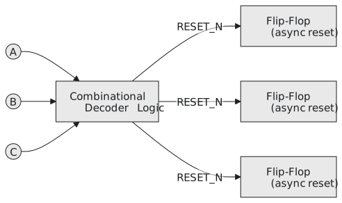
During normal operation one input changes between two states in which the reset should stay inactive, but the decoder has a static-0 hazard on that transition and the reset line dips low for a few nanoseconds. Every flip-flop in the machine resets. The transaction in progress is lost and the machine starts again.
It does not show in RTL simulation, because there are no delays there. It shows in silicon, at temperature, on a pattern that may be rare on the bench and common in the field. The consequences range from a protocol error to lost data.
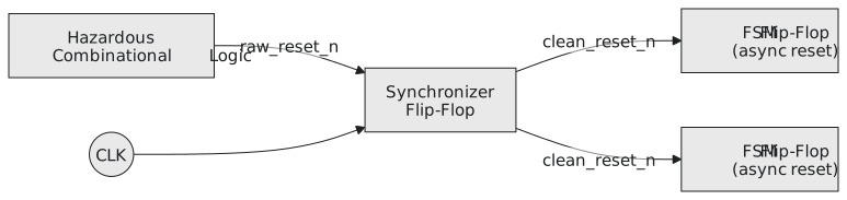
Two fixes. Make the decoder hazard-free with the procedure from the last article. Or, better, register the reset (Figure 2): a flip-flop samples the raw signal at the clock edge, after the glitch has gone, and the state machine gets a clean reset one cycle later. Then check what drives the synchroniser’s own reset, because if that is combinational too the problem has only moved.
The gated clock
A low-power design stops the clock to idle registers by ANDing it with an enable. If the enable comes from combinational logic, a glitch on it while the clock is high produces a falling and then a rising edge on the gated clock: a spurious clock edge that clocks garbage into every register in the domain (Figure 3).
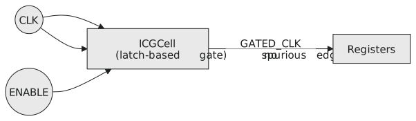
The fix is an integrated clock-gating cell from the library. It contains a latch that is transparent only while the clock is low, so the enable can only change the gated clock during the low phase, when the registers are not listening. Any glitch on the enable while the clock is high is blocked. Synthesis and lint tools flag a bare AND gate on a clock as an error precisely because this failure is so well known, and a large SoC has thousands of these cells, every one of them an ICG cell.
The bus fight
Several tri-state drivers share a bus, each with an output enable. If two are enabled at once with opposite values, there is a direct path from supply to ground through the two drivers. If the enables come from combinational logic with hazards, the outgoing driver can glitch back on while the incoming one is already on. Current spikes, the value on the bus is corrupted, and in a bad case a driver is damaged. Memory and peripheral datasheets specify enable non-overlap times for exactly this reason.
The fix: output enables come only from registered outputs, with an explicit dead time between one driver turning off and the next turning on.
FPGA carry chains and LUT paths
On an FPGA the dedicated carry chain is several times faster than routing through lookup tables. If an expression combines a carry-chain output and a LUT-path output at the same gate, the two inputs arrive at very different times (Figure 4).
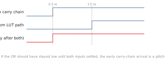
RTL simulation shows nothing. Gate-level simulation with the SDF delays from place and route shows the pulse. If the output is a synchronous signal and static timing analysis passes, it is harmless. If it drives something asynchronous, it is a bug. The remedy is either to register the output or to constrain the two paths to similar lengths. The single most effective habit in FPGA design is to have no asynchronous outputs at all: every signal that leaves the chip or crosses a clock domain comes from a flip-flop.
The synchronous design principle
All four cases have the same shape: a signal sampled without the protection of a clock edge. All four fixes put a flip-flop, or a latch-based clock gate, between the hazardous logic and the sensitive load. That is the principle:
In a fully synchronous circuit, if every flip-flop’s D input meets setup and hold at every clock edge, every glitch in the combinational logic between flip-flops is harmless.
A flip-flop looks at D at one instant, the clock edge. If
$$t_{CQ} + t_{comb,max} + t_{setup} \leq T_{period}$$
then D has settled before the edge, and anything that happened earlier is invisible (Figure 5). The hazards are still in the logic; nothing sees them.
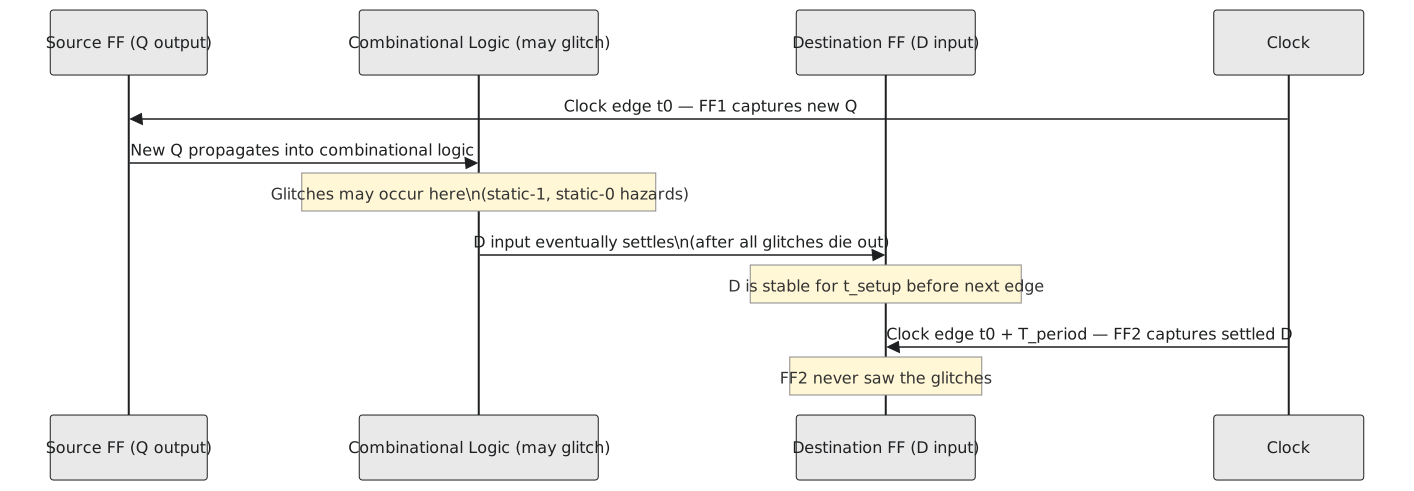
This turns a continuous-time problem, analysing every possible glitch, into a discrete one, does the data arrive before the edge, and the second is exactly what static timing analysis proves.
Where it does not reach
The principle has conditions, and they fail in known places: a corrupted clock, from crosstalk or excessive skew; asynchronous inputs that bypass synchronisers; output pins driven by combinational logic; clock gating done with a bare gate; a multi-cycle path wrongly declared as single-cycle in the timing constraints, so that the tool passes a path that is really late; and asynchronous reset pins, as in the first failure above.
What the tools see
RTL simulation has no delays. It confirms the function and cannot show a hazard. A clean RTL simulation is necessary and not sufficient.
Gate-level simulation with SDF annotation uses the real delays of the placed design. Glitches appear as narrow pulses. It is slow and needs a synthesised netlist, and it is the reference method for hazard detection.
Static timing analysis (PrimeTime, Tempus, or the FPGA vendor’s tool) checks every path against setup and hold. It does not simulate glitches; it proves that, for synchronous paths, they cannot matter.
Structural lint (SpyGlass and similar) flags combinational logic driving resets, clock enables and asynchronous loads, which tells you where to look without simulating anything.
A complete flow uses all of them.
Module 2 in review
Adders. From the half adder, two gates, to the full adder, to the ripple-carry chain whose delay grows with width, to carry lookahead with its generate and propagate signals, to carry select with its square-root delay, and to the prefix adders in real processors. Each step was a response to the previous one’s limit.
The ALU. XOR gates turned the adder into a subtractor; the four flags reported on the result; a set of parallel units and an output mux made the ALU that sits in every processor, and the flags became the condition codes that every branch reads.
Multipliers and shifters. Long multiplication became an array of AND gates and adder rows; the carry-save adder let the rows be reduced in parallel in a Wallace tree; a constant shift turned out to be wiring, and the barrel shifter made a variable shift a fixed number of mux stages.
Hazards. A correct expression with real delays can glitch. The Karnaugh map from Module 1 shows where, a redundant term fixes it, two-level logic rules out dynamic hazards, and the synchronous principle makes the whole problem one of timing.
Everything in Module 1 was used here: maps for minimisation and then for hazard detection, two’s complement in the subtractor and the flags, De Morgan in the NAND forms, the adder and mux blocks throughout.
Self-check
Before Module 3, you should be able to: derive the half and full adders from truth tables; compute a ripple-carry adder’s delay; write the carry-lookahead equations for $C_1$ to $C_3$; explain carry select and its delay; choose an adder for a given target and clock; build an adder/subtractor with XOR gates; implement the four flags; derive signed and unsigned greater-than from the flags; draw the partial products of an $N \times N$ multiply; explain the carry-save adder and the Wallace tree; give a concrete example of LSR against ASR on a negative number; design one barrel-shifter stage; find a static-1 hazard on a map and add the bridging term; state the synchronous design principle; and name three places where hazard removal is compulsory even in a synchronous design.
Practice Exercise
Problem 1. A combinational block has a static-1 hazard on one transition, and its output drives three things: the D input of a flip-flop on a 100 MHz clock (glitch 500 ps, setup 200 ps); a bare AND gate gating a 50 MHz clock; and the output enable of one of four tri-state bus drivers. For each, is there a real failure, and what is the fix?
Solution
Flip-flop D input: the clock period is 10 ns and the glitch happens as the logic settles, long before the sampling window. If timing is met, no failure. Nothing to do beyond normal timing analysis.
Bare clock gate: a dip on the enable while the clock is high makes a spurious clock edge. Real failure. Replace the AND gate with an ICG cell, and make the enable hazard-free as well.
Output enable: a dip turns the driver off and on again, briefly floating the bus or, during a handover, overlapping with the next driver. Real failure. Register the enable and enforce dead time between drivers.
Problem 2. From memory, write the full adder’s sum and carry; the overflow flag in terms of the operand and result sign bits; the hazard-free form of $F = AC + BC’$; and the generate and propagate signals.
Solution
$S = A \oplus B \oplus C_{in}$ and $C_{out} = AB + AC_{in} + BC_{in}$.
$V = A_{n-1}B_{n-1}\overline{S_{n-1}} + \overline{A_{n-1}},\overline{B_{n-1}}S_{n-1}$: two positives giving a negative, or two negatives giving a positive.
$F = AC + BC’ + AB$.
$G_i = A_iB_i$ and $P_i = A_i \oplus B_i$.
Every circuit so far has been combinational: the output depends only on the present inputs, with no memory of what came before. Module 3 adds memory. A flip-flop holds its value between clock edges, and from that one element come counters, shift registers, state machines and, eventually, processors. It starts with the simplest memory element of all, the SR latch.