What a Hazard Is
The last section of Module 2 is about something that affects every circuit in the module. Suppose you design a circuit for $F = AC + BC’$. The expression is right, the truth table checks, the simulation passes, and then in silicon, now and then, it gives the wrong answer for a fraction of a nanosecond. That is a hazard, and it comes from the one thing Boolean algebra leaves out: gates take time.
I have seen these cause real failures on real boards, and they are hard to find, because they never show up in the simulator you use during design. This article explains why they happen, the three forms they take, and which situations make them dangerous. The next articles show how to find and remove them.
Delay along different paths
Every gate has a propagation delay, tens of picoseconds in a modern process, and different for an inverter, an AND and an XOR. When an input changes, the effect travels through the circuit along every path from that input to the output, and each path has its own total delay. If two paths from the same input to the same output differ in delay, there is a window during which the output has seen the new value along the fast path but not yet along the slow one. In that window the circuit is in an inconsistent state, and its output can be wrong.
The final output is correct. Once everything has settled, the value is what the algebra says it should be. The problem is the transient before settling.
An example
Take $F = AC + BC’$ with $A = 1$ and $B = 1$, and let $C$ fall from 1 to 0.
Before: $AC = 1$, so $F = 1$. After: $BC’ = 1$, so $F = 1$. The output should stay at 1 throughout.
Now follow the gates. $C$ reaches the upper AND gate directly, and reaches the lower AND gate through an inverter. When $C$ falls, the upper AND gate switches off after one gate delay. The lower AND gate switches on only after the inverter delay plus one gate delay. For one inverter delay, both AND gates are off and $F$ drops to 0 (Figure 1).
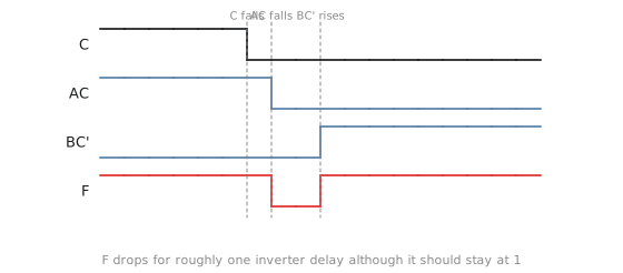
The glitch is about as wide as the inverter is slow, perhaps 30 to 50 ps. Whether that matters depends on what is listening.
Three kinds
A hazard is an output transition that should not be there: either the output changes when it should have stayed still, or it changes more than once when it should have changed once.
A static-1 hazard is an output that should stay at 1 but dips to 0. That is the example above.
A static-0 hazard is an output that should stay at 0 but rises to 1. It is the same thing in a product-of-sums circuit.
A dynamic hazard is an output that should change once but changes three or more times before settling. These need at least three levels of logic and get their own article.
When a glitch matters
A glitch is only a problem if something downstream reacts to it. That depends entirely on what is connected and when it looks.
Dangerous: a latch, which is transparent while enabled and passes the glitch straight into its stored value; an asynchronous set or reset pin, which resets the flip-flop; anything edge-sensitive that is watching the signal, such as a counter enable or an event detector, which sees an extra edge; a handshake or valid signal to another block; a pin leaving the chip, where the external device has no idea about your timing; and a clock enable or gated clock, which produces a spurious clock edge. That last one is among the most common hazard failures in practice.
Safe: the D input of a flip-flop in a synchronous design where timing is met. The flip-flop only looks at D at the clock edge, and if the setup time is satisfied, every glitch has died out before then.
Beginners sometimes argue that the simulator showed no glitches, so the circuit is fine. A zero-delay simulation models gates as instantaneous and cannot show a glitch. Glitches appear only in gate-level simulation with timing annotation, or in hardware.
The synchronous defence
The main protection is synchronous design: every signal feeding a flip-flop is stable before the clock edge, and every signal that might glitch is sampled only at a clock edge.
The argument is simple. A flip-flop captures D at the clock edge and ignores it otherwise. After the edge, the new Q value propagates through the combinational logic to the next D input, and during that propagation there may be glitches. The next clock edge comes only after the logic has settled, and the setup constraint,
$$T_{period} \geq t_{CQ} + t_{comb} + t_{setup}$$
guarantees it, provided $t_{comb}$ is the worst-case delay including all the settling. If timing is met, the flip-flop never sees a glitch. The glitches are still there inside the logic; they are just invisible to anything that matters.
This is why synchronous design dominates. It turns “will there be a glitch?” which is a hard analogue timing question, into “does the data arrive before the clock edge?” which static timing analysis answers exactly.
Where synchronous design does not reach
Some parts of a design sit outside the clocked discipline and stay hazard-sensitive whatever you do elsewhere: reset networks driven by combinational logic, clock enables that are not proper clock-gating cells, output pins driven by combinational logic, and asynchronous inputs from buttons, other chips or other clock domains. These are exactly the boundaries between synchronous and asynchronous behaviour, and they are where hazard analysis has to be done by hand. They are also where bugs are hardest to reproduce in simulation.
| cause | different delays along different paths |
| static-1 | dips to 0 when it should stay 1 |
| static-0 | rises to 1 when it should stay 0 |
| dynamic | three or more transitions instead of one |
| dangerous | latches, async resets, pins, clock enables, handshakes |
| safe | flip-flop D input with timing met |
Practice Exercise
Problem 1. For $F = A’B + AB’$, is a hazard possible when $A$ and $B$ change together from 00 to 11? What about $A$ alone changing from 0 to 1 with $B = 0$?
Solution
Hazards are defined for single-variable changes, so the first case is outside the definition, but note that in practice the two inputs will not change at exactly the same instant, and the circuit passes through 01 or 10, where $F = 1$, on its way from 00 to 11, where $F = 0$. That gives a real pulse on $F$, which is a function hazard rather than a logic hazard: it is in the function itself, and no amount of extra logic removes it.
For $A$ rising with $B = 0$, $F$ goes from 0 to 1. That is a change, so a static hazard does not apply, and a two-level circuit cannot have a dynamic hazard. The output makes one clean transition.
Problem 2. A combinational block drives the write enable of an SRAM. A colleague says the Boolean expression is correct so it is fine. What else is needed?
Solution
A correct expression does not mean a glitch-free output. The write enable is sampled asynchronously by the memory, and a few nanoseconds of spurious assertion corrupts a location. You need to find every single-variable transition on which WE should stay inactive, check on a map whether each such pair of adjacent cells is covered by one term, add redundant terms where it is not, and confirm with a gate-level simulation with timing annotation, because synthesis may restructure the logic. Better still, register the signal.
In the next article we look at static hazards in detail and see that the Karnaugh map, which we used for minimisation in Module 1, also shows exactly where the hazards are.