What an ALU Is
We can add and subtract. A processor’s instruction set wants more than that: AND two registers, OR them, XOR them, invert one, compare two values, copy a register unchanged. It wants all of these from one circuit, chosen at run time by whatever instruction arrives. That circuit is the arithmetic logic unit, and this article is about how it is put together. The pattern has not changed much since 1970, and it comes down to one idea: compute every operation at once, and select the one you asked for.
The interface
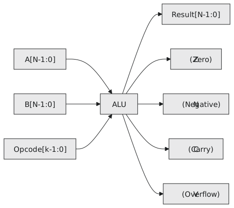
Before designing anything, fix the interface. The interface is a contract with the rest of the processor; everything inside it is an implementation detail.
| Signal | Width | Direction | Meaning |
|---|---|---|---|
| A | N | in | first operand |
| B | N | in | second operand |
| opcode | k | in | operation select, up to $2^k$ operations |
| result | N | out | the computed value |
| Z | 1 | out | result is zero |
| N | 1 | out | result is negative (signed) |
| C | 1 | out | carry, or no-borrow |
| V | 1 | out | signed overflow |
The opcode width $k$ is a design decision: two bits give four operations, three give eight, four give sixteen. The flags are a separate reporting channel alongside the result. They go into a status register that conditional branch instructions read.
Which operations
Not every operation belongs in the ALU. The set is chosen to serve the instruction set architecture, but the same groups appear almost everywhere.
Arithmetic. ADD, SUB, and usually ADC, add with carry, which brings the carry flag from a previous addition in as the carry-in and is what makes multi-word arithmetic possible.
Logic. AND for masking, OR for setting bits, XOR for toggling and comparing, NOT for inversion. Each works bit by bit with no interaction between positions.
Pass-through. Result = A, and sometimes result = B. These look trivial but they are how a register-to-register move goes through the datapath without needing a separate bypass.
Compare. CMP is SUB with the result thrown away: it exists only to set the flags. The hardware is identical to SUB; the difference is that the register write is suppressed outside the ALU.
Shifts. Shift by one is sometimes in the ALU and sometimes in a separate shifter. We build a proper barrel shifter in section 2.3.
One circuit for all of them
The circuits for $A + B$, $A \cdot B$ and $\bar{A}$ are completely different gate networks. How do you get one block that does all three?
You could imagine rewiring the gates according to the opcode. At the gate level that is impractical; nothing rewires in nanoseconds.
What every real ALU does instead is build all the operation circuits, run all of them all the time on the same inputs, and put a multiplexer on the end that passes only the one the opcode names. The rest are computed and discarded. Figure 2 shows the shape.
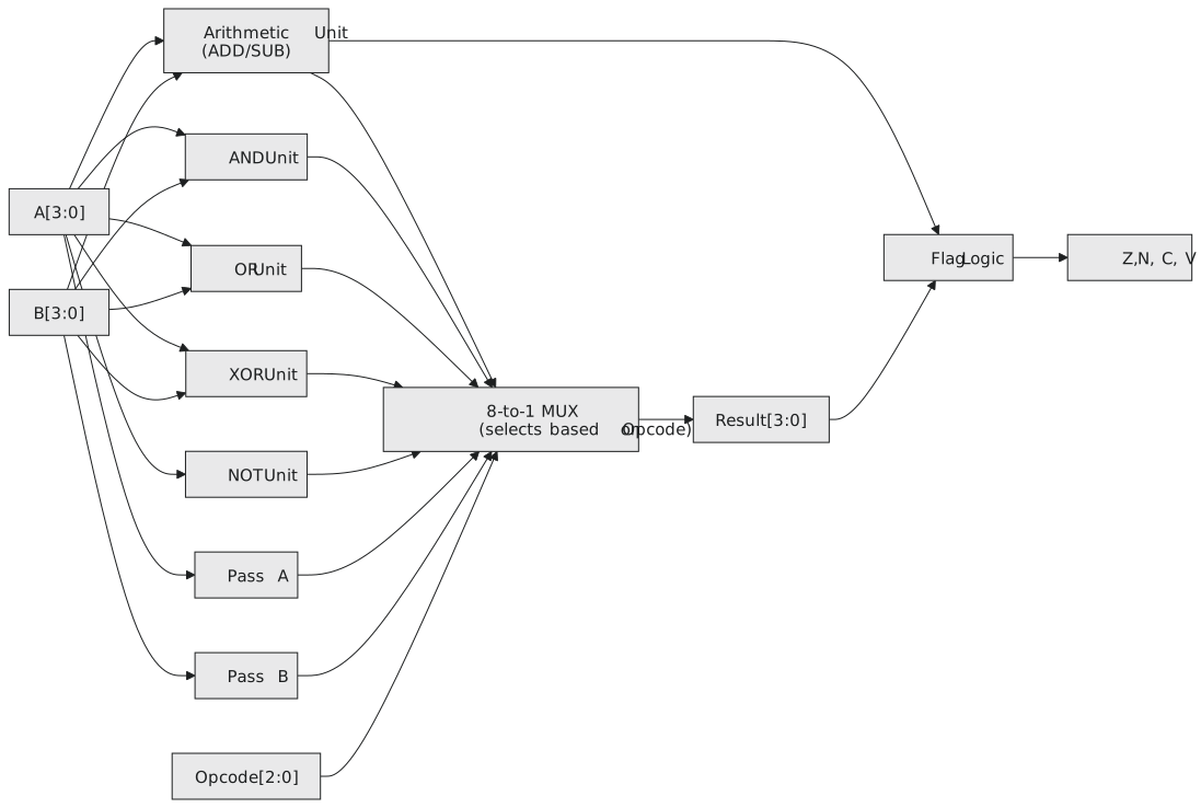
This works for three reasons. The mux adds only a gate delay or two, which is small next to the adder. The extra area is affordable, since a 4-bit AND unit next to a 4-bit adder is a handful of gates. And the result is always ready after the same fixed delay, whatever the operation, which makes pipeline timing simple.
The cost is power. The units whose results are discarded still switch. On a processor that matters, and it is why modern CPUs gate the clock or the power to units that are idle.
The same “compute all, select one” pattern is everywhere in digital design once you look for it: the carry-select adder, the lookup table in an FPGA, a branch predictor that follows both paths.
The 74181
The Texas Instruments SN74181, from 1970, was the first complete ALU on one chip: a 4-bit unit with carry lookahead and, remarkably, 32 selectable functions. It has four function-select inputs S3 to S0 and a mode input M (0 for arithmetic, 1 for logic), so $2^5 = 32$ combinations. A few rows of its function table:
| M | S3 | S2 | S1 | S0 | Function |
|---|---|---|---|---|---|
| 1 | 0 | 0 | 0 | 0 | NOT A |
| 1 | 0 | 1 | 1 | 0 | A XOR B |
| 1 | 1 | 0 | 0 | 0 | NOR |
| 1 | 1 | 1 | 1 | 0 | B |
| 0 | 1 | 0 | 0 | 1 | A plus B |
| 0 | 0 | 1 | 1 | 0 | A minus B |
| 0 | 1 | 1 | 0 | 0 | A plus (A AND B) |
| 0 | 0 | 0 | 0 | 0 | A |
Some of the 32 are the everyday operations and some are oddities like “A plus (A and B)” that fall out of enumerating every combination of the control inputs through the gate network. That is a feature of the select architecture: you get the in-between functions whether you want them or not.
The 74181 went into minicomputers such as the PDP-11 and into many other machines of the decade, and several could be chained with the 74182 lookahead generator into 8-, 16- or 32-bit ALUs. Its datasheet is still available, and the function table repays a few minutes of study.
When an ARM processor executes ADD R0, R1, R2, the values of R1 and R2 appear on the ALU’s A and B inputs, the decoded opcode drives the select lines, and the result comes out a few gate delays later. The gap between the 4-bit ALU we build next and that one is scale and optimisation, not a different design.
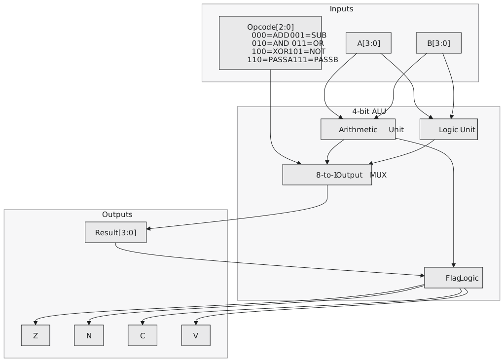
The opcode drives the output mux and the adder’s add/subtract control. Everything else computes unconditionally.
Practice Exercise
Problem 1. An 8-bit microcontroller ISA needs ADD, SUB, AND, OR, NOT A, shift left by 1, shift right by 1 and CMP. How many distinct hardware operations is that, how many opcode bits are needed, and what are the blocks?
Solution
CMP is SUB with the write-back suppressed, so it is not a separate ALU operation. That leaves seven: ADD, SUB, AND, OR, NOT, SHL, SHR. Seven operations need $\lceil \log_2 7 \rceil = 3$ opcode bits, which gives eight slots and one spare, perhaps for XOR or pass-through.
Blocks: an adder/subtractor for ADD and SUB; a logic unit computing AND, OR and NOT in parallel; a shift unit for SHL and SHR; an 8-to-1 output mux driven by the opcode; flag logic from the result and the adder’s carries.
Problem 2. Why do all the units compute on every cycle, and what is one advantage and one disadvantage compared with a hypothetical design that computed only what was needed?
Solution
Combinational logic has no off switch; whatever is on the inputs propagates through every network at once. The advantage is fixed, predictable latency: the ALU always takes the same time regardless of operation, which makes pipeline timing simple. The disadvantage is wasted dynamic power in the units whose results are discarded, which is why processors add clock gating or power gating around idle units.
That is the plan: list the operations, assign opcodes, build every unit, select with a mux. In the next article we carry it out in full and build a 4-bit ALU with eight operations, gate by gate.