Building a 4-Bit ALU
The last article gave the plan; this one carries it out. By the end you will have a 4-bit ALU with eight operations, every unit specified, every signal named, every gate counted, and one operation traced through it from inputs to flags. There are four steps: the arithmetic unit, the logic unit, the output mux, and the flag logic. Then we put them together.
The specification
Eight operations chosen by a 3-bit opcode $S_2 S_1 S_0$:
| Opcode | Operation | Result |
|---|---|---|
| 000 | ADD | $A + B$ |
| 001 | SUB | $A - B$ |
| 010 | AND | $A$ AND $B$, bitwise |
| 011 | OR | $A$ OR $B$ |
| 100 | XOR | $A$ XOR $B$ |
| 101 | NOT | NOT $A$, B ignored |
| 110 | PASSA | $A$ |
| 111 | PASSB | $B$ |
Inputs $A[3:0]$, $B[3:0]$ and $S[2:0]$; outputs $R[3:0]$ and the flags Z, N, C, V.
Step 1: the arithmetic unit
This is the adder/subtractor from the last two articles, with $S_0$ as the sub signal. Note that ADD is 000 and SUB is 001, so $S_0$ alone tells the adder which to do.
- Four XOR gates: $B’_i = B_i \oplus S_0$.
- Carry-in to FA0: $S_0$.
- A 4-bit ripple-carry adder.
Outputs: the 4-bit result, the carry out of FA3 (call it ArithCout) for the C flag, and the carry into FA3 ($c_3$) for the V flag.
The unit computes on every opcode; its result is only selected for 000 and 001. Gate count: four XORs plus four full adders at five gates each, about 24 gates.
Step 2: the logic unit
Four bitwise operations, all computed at once, no interaction between bit positions:
- AND: $A_i \cdot B_i$, four gates
- OR: $A_i + B_i$, four gates
- XOR: $A_i \oplus B_i$, four gates
- NOT: $\bar{A_i}$, four gates, B not connected
Sixteen gates, each output one gate delay from the inputs. The logic unit is always the fastest path through an ALU. The arithmetic unit, with its carry chain, is always the critical path, and that is where timing effort goes.
Step 3: the output mux
An 8-to-1 mux, four bits wide, selected by $S[2:0]$:
| Input | Signal | Opcode |
|---|---|---|
| 0 | arithmetic result | 000 |
| 1 | arithmetic result | 001 |
| 2 | AND | 010 |
| 3 | OR | 011 |
| 4 | XOR | 100 |
| 5 | NOT | 101 |
| 6 | $A$ | 110 |
| 7 | $B$ | 111 |
Inputs 0 and 1 are the same wires: the adder has already done the right thing according to $S_0$.
A 4-bit-wide 8-to-1 mux is four 1-bit 8-to-1 muxes sharing the select lines. Each can be a 3-to-8 decoder, eight AND gates and an 8-input OR, or a tree of 2-to-1 muxes three levels deep. Either way it is about three gate delays and, at roughly 80 gate equivalents for the four bits, it is the largest single piece of the ALU.
Step 4: the flags
Z: $\overline{R_3 + R_2 + R_1 + R_0}$, a NOR tree on the mux output, two gate levels.
N: $R_3$, a wire.
C: ArithCout, a wire from FA3. It is only meaningful for ADD and SUB. A minimal design wires it straight through and lets the instruction set define when it is valid; a more careful one gates it with $\overline{S_2}$ or similar.
V: $c_3 \oplus \text{ArithCout}$, one XOR. Also meaningful only for ADD and SUB.
About five gates for all four flags.
The whole thing
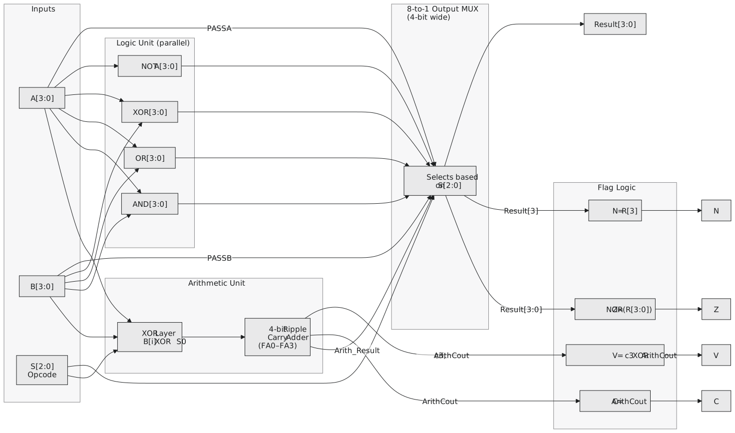
Tracing SUB: 7 − 3
Opcode 001, $A = 0111$, $B = 0011$.
XOR layer. $S_0 = 1$, so $B’ = 1100$ and the carry-in is 1. The adder computes $0111 + 1100 + 1$.
| Bit | A | B' | Cin | Sum | Cout |
|---|---|---|---|---|---|
| 0 | 1 | 0 | 1 | 0 | 1 |
| 1 | 1 | 0 | 1 | 0 | 1 |
| 2 | 1 | 1 | 1 | 1 | 1 |
| 3 | 0 | 1 | 1 | 0 | 1 |
Arithmetic result $0100$, $c_3 = 1$, ArithCout = 1.
Logic unit, computed and not selected: AND $0011$, OR $0111$, XOR $0100$, NOT $1000$.
Mux. Opcode 001 selects input 1: $R = 0100$.
Flags. $Z = \overline{0 + 1 + 0 + 0} = 0$. $N = R_3 = 0$. $C = 1$, meaning no borrow, $7 \geq 3$. $V = 1 \oplus 1 = 0$.
Result 4, flags Z = 0, N = 0, C = 1, V = 0. All correct.
Gate count
| Unit | Gates |
|---|---|
| XOR layer | 4 |
| four full adders | 20 |
| logic unit | 16 |
| 8-to-1 mux, 4 bits wide | about 80 |
| flags | 5 |
| total | about 125 |
An eight-operation 4-bit ALU is around 125 gates. The mux is well over half of it.
One mistake I have seen more than once when people build the arithmetic unit: connecting $S_0$ to the carry-in and forgetting the XOR layer on B. That computes $A + B + 1$, not $A - B$. Both halves are needed, the inversion and the extra 1. Trace both paths with sub = 1 before you trust the design.
Timing
Using two gate delays per full adder on the carry path:
| Path | Delay |
|---|---|
| A or B to a logic unit output | 1 |
| $S_0$ or B through the XOR layer | 1 |
| carry chain through FA0 to FA3 | 8 |
| $c_3$ and ArithCout to V | 1 |
| top sum bit through the mux | 1 + 3 |
| mux output to Z | 2 |
| arithmetic path to Z, worst case | about 15 |
| logic path to Z | 1 + 3 + 2 = 6 |
The arithmetic path is well over twice the logic path, and it is the carry chain that makes it so. Replacing the ripple-carry adder with a carry-lookahead adder is the single change that shortens the ALU most.
Practice Exercise
Problem 1. Trace opcode 010 (AND) with $A = 1011$, $B = 0110$. Give the result and the flags.
Solution
The arithmetic unit still runs, with $S_0 = 0$: $B’ = 0110$, carry-in 0, result $0001$ with ArithCout = 1 and $c_3 = 1$. It is not selected.
Logic unit: AND $= 0010$, OR $= 1111$, XOR $= 1101$, NOT $= 0100$.
The mux selects AND: $R = 0010$ (2).
Z = 0, N = 0. C and V are not meaningful for a logic operation; the wires carry whatever the unused adder produced, and the instruction set says to ignore them.
Problem 2. What is the worst-case delay from a B input to the V flag, and which gates are on the path?
Solution
B goes through the XOR layer (1), then along the carry chain through FA0, FA1, FA2 and FA3 (2 each, 8), producing ArithCout, and then through the V XOR (1): about 10 gate delays. The gates are the B-input XOR, then in each full adder the AND and OR of the carry path, then the final XOR. The other input to the V gate, $c_3$, arrives two gate delays earlier, so ArithCout sets the timing.
The ALU is built. The four flag bits at the bottom of the diagram are, in a sense, more important than the result, because they are what makes conditional execution possible. The next article looks at them properly: what each one means, and how a processor turns them into signed and unsigned comparisons.