CTS Across Gated Clock Domains
The previous article established that an ICG cell is a clock-network element, not a data path element. This one goes a step further. Everything downstream of that ICG is, in a real sense, its own clock domain, and treating it as a lesser appendage of the main tree rather than a first-class structure with its own skew and latency analysis is a genuine, documented way real designs pick up timing bugs.
The enable signal has timing too
Here is the detail that is easy to miss. The ICG’s GATE input is itself a signal with real setup and hold requirements relative to the clock it is gating. The latch inside the cell has to capture GATE cleanly, on the correct clock phase, or the whole point of the latch, avoiding a glitch when the enable changes near an edge, is defeated. So the path that generates the enable, wherever it comes from, most likely a control FSM output, has its own timing check that did not exist before the ICG entered the design:
$$\text{Enable setup slack} = T_{clk} - (t_{comb,\text{en path}} + t_{setup,\text{ICG latch}} + \text{skew}_{\text{en to ICG}})$$
That is the same setup machinery from Section 5.1 applied to a new endpoint, the ICG’s GATE pin instead of a flop’s D pin. If the enable arrives late, or the ICG’s local clock latency is skewed unfavourably relative to the register that generates it, the gating decision itself is captured wrongly. That is a different failure from anything earlier in this module, and it exists only because gating exists.
Skew budgets do not automatically match across the boundary
Consider two flops, one inside the gated domain downstream of the ICG and one in the ungated part of the tree, on a path that crosses between them. Section 5.1’s skew definition still applies, but the gated register’s latency now includes both the ordinary tree latency up to the ICG and whatever the ICG itself contributes as an active element in the path:
$$L_{\text{gated register}} = L_{\text{tree to ICG}} + t_{\text{ICG}} + L_{\text{ICG to register}}$$
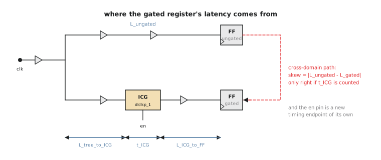
If TritonCTS balances the ungated part carefully but treats the gated sub-tree as an unremarkable branch, not counting the ICG’s insertion delay as a real contributor, any path crossing between a gated and an ungated register ends up with skew nobody verified, because the tool’s accounting silently underestimated one side.
That is what “first-class” means here. TritonCTS’s clustering and balancing has to include the ICG’s delay as a real term in every downstream register’s latency, exactly as if it were another buffer in the tree, which from a timing analysis standpoint it functionally is. A tool, or a person reading a report, that mentally sets the ICG’s delay to zero “because it is just an enable gate” is making the same idealisation error Section 5.4 spent a whole article warning against with clock latency in general. Gating is a low-power feature, and it is tempting to assume it is timing-neutral. It is not. It adds an active element to the clock network, a new timing check on the enable path, and a domain-boundary skew question, and none of that scrutiny is optional.
What this means for the capstone
None of it changes the mechanics from Sections 5.3 and 5.4. Clustering, buffered tree construction and hold risk on short paths all still apply. It adds one more category of path to check specifically: anything crossing between the gated baud generator domain and the rest of the UART, control signals telling the gated domain to wake up and status coming back out of it, needs its skew and hold analysis to correctly include the ICG sitting in one side’s clock path. The next article’s capstone runs exactly this check.
Practice Exercise
A control FSM asserts a gating enable that reaches an ICG’s GATE pin. List the two distinct timing checks this signal path now requires that would not exist in a fully ungated version of the same design, and say what each verifies.
Solution
- A setup check on the enable path itself, from the FSM’s enable-generating register to the ICG latch, verifying the gating decision is captured before the relevant clock edge, using the enable setup equation above.
- A skew and hold check on any path crossing between the gated and ungated domains, verifying that a register inside the gated sub-tree and one outside it have correctly accounted-for relative latency, including the ICG’s own insertion delay rather than an idealised zero.
Neither has an equivalent in an ungated design, because neither the ICG nor the domain boundary it creates would exist.
Every concept this section needs is in place. The final article runs CTS for real on a gated variant of the UART’s baud generator and shows what the resulting tree, ICG included, actually looks like.