Defining Skew and Latency
The previous article used latency and skew loosely enough to get the intuition across: a longer wire takes longer, so two edges arrive apart. That is exactly the kind of looseness a CTS report will not tolerate. TritonCTS’s summary, OpenSTA’s clock reports and every conversation you will have with another physical designer use these two words with specific meanings. Get them right now, because the rest of this module and Module 7’s timing closure assume you have them cold.
Clock latency
Clock latency is the time a clock edge takes to travel from the clock’s defined source point to a specific register’s clock pin. It has two components worth naming separately. Source latency is the delay from the actual clock generation point, an external pad or a PLL, to the point OpenSTA treats as the clock definition point, the one named in create_clock. Early in a flow this is usually modelled rather than measured. Network latency is the delay through the distribution network itself, the buffers and wires CTS builds, from that definition point out to each individual register.
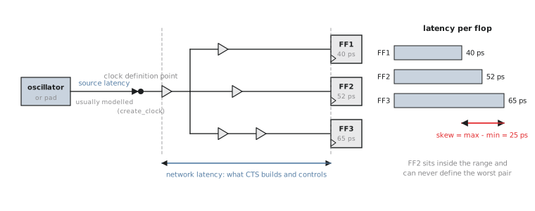
When people say clock latency during CTS and post-CTS work they almost always mean network latency, because that is the part CTS controls and the part that changes as the tree gets built. This course follows that convention from here on. Latency means network latency unless stated otherwise.
Clock skew
Clock skew is the difference in network latency between two registers on the same clock domain. Skew is always a property of a pair. There is no such thing as the skew of flop A in isolation, only the skew between A and B. When a report gives one skew number for a whole design it means the worst-case pairwise skew, the largest latency difference between any two registers being compared.
$$\text{Skew}_{A,B} = |L_A - L_B|$$
$$\text{Worst-case skew} = \max_{i,j}\left(|L_i - L_j|\right) = L_{\max} - L_{\min}$$
That second formula is a genuinely useful shortcut. For any group of registers, the worst-case pairwise skew is the highest latency minus the lowest. You never need to check every pair.
Three flops
Suppose a post-CTS report gives these three network latencies on one clock domain:
| Flip-flop | Network latency |
|---|---|
| FF1 | 40 ps |
| FF2 | 65 ps |
| FF3 | 52 ps |
Worst-case skew is the spread:
$$65,\text{ps} - 40,\text{ps} = 25,\text{ps}$$
FF3’s 52 ps never had to be compared against the other two. It can only sit inside the range set by the max and min, so it can never be part of the worst-case pair. This is why real CTS reports usually publish min latency, max latency and skew as three numbers rather than a full pairwise table. Those three contain everything you need. And a tool like TritonCTS is not just measuring skew after the fact. It is actively trying to minimise worst-case skew, or hit a target, as it decides where to place buffers and how to balance branches. Section 5.3 opens up how.
One confusion worth heading off. A design where every flop has 200 ps of latency has zero skew. Every edge is late by the same amount, which is harmless to setup and hold, because timing checks only ever care about the relative difference between a launching and a capturing register’s clock arrival, never the absolute value. High latency by itself is not a timing problem. High skew is.
Practice Exercise
A clock domain reports four latencies: FF_A = 30 ps, FF_B = 58 ps, FF_C = 44 ps, FF_D = 71 ps. What is the worst-case skew, and which pair defines it?
Solution
$$71,\text{ps} - 30,\text{ps} = 41,\text{ps}$$
The defining pair is FF_D (71 ps, the latest) and FF_A (30 ps, the earliest). FF_B and FF_C sit inside that range and cannot contribute a larger difference than the max-minus-min pair already does.
You can now define and compute skew precisely. The next article connects that number directly to the setup equation from the Verilog course’s STA lesson, and shows how many picoseconds of skew a path can absorb before it stops passing.