Why a Single Wire Fails
Module 5 starts with a drawing you have been trusting since the first module of the Verilog course. Somewhere on every schematic since then there is a little clock symbol with a wire fanning out to every flip-flop, drawn exactly the same way a logic signal is drawn: a clean line that connects things. Implicit in that drawing is an assumption you have leaned on for nine modules of physical design and verification. Every flip-flop sees the clock edge at the same instant.
That assumption is not a simplification. It is a fiction, and the moment the design is placed on real silicon the fiction stops being harmless.
A wire is an RC network
A schematic wire is a mathematical abstraction, an ideal zero-delay connection between two points. A routed metal wire is a physical object with resistance and capacitance spread along its length. Every extra micron adds a little more resistance and a little more capacitance to ground, and an RC network takes real time to charge and discharge. That time is the wire’s propagation delay, and it depends on how far the wire has to run.
Now place two flops on a real floorplan. One sits close to wherever the clock enters the design. The other sits across the die, because that is where placement decided it needed to go to keep the data nets short. Placement, as Module 4 showed, optimises connectivity and density and has no built-in reason to respect clock symmetry. The clock reaches the near flop quickly. It reaches the far one only after propagating through a much longer, much more resistive and capacitive wire.
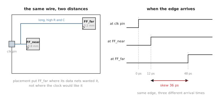
Both flops are driven by “the same clock”. Neither receives it at the same time. That difference, two supposedly identical edges arriving at different instants, is the single fact clock tree synthesis exists to manage. Left unmanaged, on a real die at a real frequency, an unbuffered single wire simply does not work. The far flops would be so late relative to the near ones that the design would fail timing before you even got to consider the logic between registers.
Every stage so far, synthesis, floorplanning and placement, has used an ideal clock with zero network delay, purely because CTS has not happened yet. That was fine as a placeholder. It stops being fine the instant you need a real timing number, which is why this module comes before routing rather than after. The clock tree has to exist before the design can be routed and its real timing evaluated.
Your first skew number
Let me put a number on it, with an explicitly illustrative delay-per-length figure. It is not a SKY130 datasheet value, just a reasonable stand-in so the arithmetic means something: assume a routed, unbuffered clock wire contributes roughly 15 ps of delay per millimetre. Say the floorplan puts two flops at these distances from the clock pin:
| Flip-flop | Distance from clock source |
|---|---|
| FF_near | 0.8 mm |
| FF_far | 3.2 mm |
The clock’s latency to each, the time from source to that flop’s clock pin (the next article defines it formally), is distance times the delay-per-length figure:
$$L_{\text{near}} = 0.8,\text{mm} \times 15,\text{ps/mm} = 12,\text{ps}$$ $$L_{\text{far}} = 3.2,\text{mm} \times 15,\text{ps/mm} = 48,\text{ps}$$
The difference is 48 - 12 = 36 ps. That number, the spread between the latest and earliest clock arrival on the same clock domain, is skew, and you just computed one by hand from geometry alone.
Thirty-six picoseconds sounds tiny. It is not free. It comes directly out of the setup margin every register-to-register path depends on, which is the connection the next two articles build out in full. And a design that “passed timing” at synthesis says nothing about this. Synthesis-stage STA uses an ideal, zero-latency clock by construction. It is not wrong, it is simply not yet answering the question that CTS and post-CTS STA will answer.
Practice Exercise
Using the same 15 ps/mm figure, compute the latency to a flop 1.6 mm from the clock source and to a second flop 5.0 mm away. What is the arrival-time difference between them?
Solution
$$L_1 = 1.6,\text{mm} \times 15,\text{ps/mm} = 24,\text{ps}$$ $$L_2 = 5.0,\text{mm} \times 15,\text{ps/mm} = 75,\text{ps}$$
Difference: 75 - 24 = 51 ps. It is already a bigger number than the worked example, purely because the second flop sits further out. Skew scales with how physically spread out your flops are, which is exactly why large, sprawling designs have a harder CTS problem than small, compact ones.
You now have an intuitive, quantified feel for why a bare wire fails. The next article makes latency and skew precise terms, because the informal picture above will not be good enough once you need to reason about ten, or ten thousand, flip-flops at once.