Integrated Clock Gating Cells
Section 5.5 picks up a thread from Module 7 of the Verilog course, which taught you never to write assign gated_clk = clk & en; and explained that the safe alternative is an integrated clock gating cell, an ICG: a transparent latch feeding an AND gate, built to avoid the glitch a bare combinational AND creates on a clock. That lesson stopped at the logical view. This article asks the physical design question: what does that structure actually turn into, and where does it live in the design this module has been building?
From logical structure to physical cell
In the SKY130 sky130_fd_sc_hd library the ICG is a specific cell, sky130_fd_sc_hd__dlclkp_1, “D-latch clock gate, positive”. It physically contains exactly the latch-plus-AND structure from the Verilog course’s diagram. It is not a discrete latch and a discrete AND that the synthesiser wired together. It is one pre-characterised, pre-verified standard cell the PDK ships for this purpose, with three pins: CLK, GATE and GCLK.
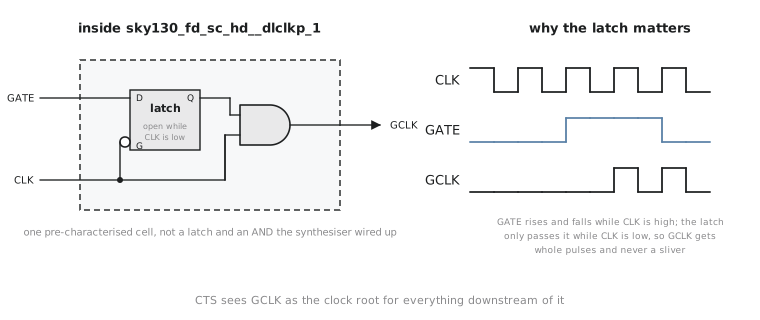
How it gets into the netlist depends on the flow. Commercial synthesis tools infer an ICG from a recognised clock-enable idiom in the RTL. In the open flow this course uses, Yosys does not infer clock gating cells, so the practical route is to instantiate the library cell directly in the RTL, which is what the capstone article two ahead does. Either way, the thing that ends up in the placed design is the same cell.
Why the ICG belongs inside the clock network
This is the distinction the Verilog course had no reason to make and this module does. An ICG is not just a gate the design happens to contain, the way an ALU’s adder or the UART’s shift register is. It is a clock-network element, structurally, and floorplanning, placement and above all CTS have to treat it as one.
Concretely, the ICG’s GCLK output drives the clock pin of every flop in its gated domain, exactly the way an ordinary clock buffer’s output does. TritonCTS has to know the cell exists and sits on the clock net, because everything downstream of it, every flop the gated clock reaches, has its latency and skew computed starting from GCLK, not from the ungated root. Treat an ICG as an ordinary logic cell on a data path and CTS never accounts for it, and every downstream latency number is wrong. This is why the physical view of gating earns its own section instead of being folded into Section 5.1. Every gated clock domain in a real design routes through one of these, and CTS treats its output as a new, local clock root.
Where this shows up in the UART
uart_top, as built in the Verilog course’s capstone, runs its baud generators continuously. They were never written with a gated enable. The final article of this section introduces a gated variant specifically to give the module’s capstone something real to run CTS against: an enable that gates the receive baud generator’s clock off while the UART sits idle, neither transmitting nor receiving. That is the activity-aware gating the Verilog course discussed in the abstract, now with a physical destination.
Gating is one of the highest-leverage low-power techniques in real ASIC design, precisely because a gated domain’s flops stop toggling entirely while gated. No edges reaching them means no switching activity and no dynamic power on that domain for as long as the gate stays closed. A chip with a handful of large, frequently idle blocks, and a UART idle between bytes is a realistic example, can see meaningful savings from gating just those blocks correctly.
Practice Exercise
List the three representations the same logical clock-gating idea passes through across this course and the Verilog course, in order from most abstract to most physical.
Solution
- The RTL-level intent (Verilog course, Module 7): a clock enable, deliberately not a raw AND gate on the clock.
- The logical ICG structure (also Verilog course, Module 7): the latch-plus-AND view that explains why the glitch is avoided.
- The physical standard cell (this article):
sky130_fd_sc_hd__dlclkp_1, sitting inside the clock network as a CTS-aware element rather than an ordinary data path gate.
You now know what an ICG cell is physically and where it sits. The next article explains why a gated sub-tree downstream of that cell cannot be bolted onto the rest of the tree as an afterthought. It needs its own skew and latency treatment.