Why "Correct at Nominal" Isn't Enough
In the previous article we saw that real chips spread around nominal. In this article we look at what that means for signoff. Imagine uart_top checked only at the typical corner. Setup slack is comfortably positive, DRC and LVS are clean, IR drop is in budget. You tape out, and months later a noticeable fraction of the returned chips fail at the target clock. Every check passed. What happened?
The typical corner is the middle, not the whole picture
Because of process variation, real chips do not all sit at typical. Some come out closer to the slow corner, with weaker transistors and longer delays; some closer to the fast corner. Supply voltage and temperature in use move them further. Figure 1 shows the picture.
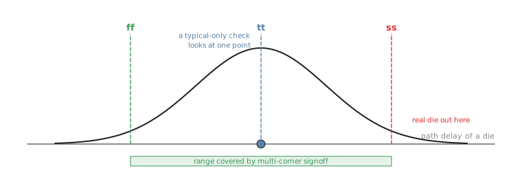
A design checked only at typical has no demonstrated margin for any chip that lands elsewhere, and many correctly made chips will land elsewhere, because that is what a distribution means. The slower half of the population is exactly where setup fails, and the faster tail is where hold fails.
This is why Module 7 signed off at several PVT corners instead of one. Margins and derating exist for the same reason: derating covers the variation between cells inside one die, which the corners do not model, and extra timing margin covers everything the models leave out.
Applying a margin by hand
Suppose a project’s signoff policy requires every path to keep a margin of 5% of the clock period on top of the reported setup slack, to cover effects the analysis does not model well. At the typical corner, the worst setup slack is $+0.42$ ns on a 10 ns clock. How much of it is real margin?
$$ \text{Required margin} = 0.05 \times 10\ \text{ns} = 0.50\ \text{ns} $$
$$ \text{Slack after margin} = 0.42\ \text{ns} - 0.50\ \text{ns} = -0.08\ \text{ns} $$
A comfortably positive-looking number becomes a small violation once the policy is applied, and this is still only the typical corner. At the slow corner the same path would be worse again. Nothing about the design changed between the two lines, only how honestly the number accounts for what the typical analysis leaves out. In practice such a policy is usually written into the constraints, for example as extra clock uncertainty, so that every report already includes it.
It is a mistake to read a comfortable typical-corner slack and treat the slow and fast corners as a formality. For judging whether a real population of chips will work, the typical corner is the least informative of the three: it tells you about the middle, and failures happen in the tails.
This is also why the PDK ships ss, tt and ff libraries. They are not an optional stress test. They are the foundry’s statement of the range a real chip can land in, and every serious design is expected to meet its targets across all of them.
Practice Exercise
A design is clean at tt (worst setup slack +0.42 ns) and at ff. At ss the worst setup slack is −0.09 ns, a small violation. A teammate argues: “It’s basically zero, and it passed at typical, let’s tape out.” What is wrong with that?
Solution
A negative slack at any signoff corner is a real violation. Process variation guarantees that some real chips will behave like the slow corner, so −0.09 ns at ss describes an actual population of chips that will miss the clock period (at the slow corner’s voltage and temperature), not a rounding artefact. “It passed at typical” is exactly the reasoning this article argues against: the slow corner does not become less real because another corner looked fine. The fix is an ECO as in Module 7, or, if the application allows it, a documented decision to specify the part at a slightly lower clock frequency.
In the last article of this module we step back and look at the whole flow, from floorplan to GDS, as one discipline aimed at manufacturability rather than a series of separate checklists.