Packaging and What Comes Back
Months after submission, a small box arrives. In this article we look at what happens before its contents answer the question this whole course has been building up to: did it work?
Dicing and packaging
The finished wafer is sawn or laser-cut along the scribe lines, the streets between die from the previous article, into individual die. Each die, or in a shuttle each copy of the shared chip, is then packaged: mounted on a substrate or lead frame, its pads connected to the package pins by bond wires or solder bumps, and sealed for protection and handling. On shuttles, the chips often come back already mounted on a small test board.
Bring-up
Bring-up is the sequence of tests a returned chip goes through the first time it is powered, as in Figure 1.
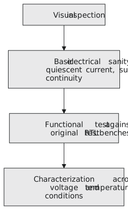
It starts with a visual inspection and basic electrical checks: are the supplies connected, and does the chip draw roughly the expected current when idle? That is the LVS connectivity check of Module 8 in physical form. Then functional testing: running the same kinds of tests used in RTL verification, now on silicon instead of in a simulator. For the UART, that means sending bytes into it and checking what comes back. Finally characterisation: running the chip across supply voltage and temperature to see how it compares with the signoff corners of Module 7.
Before reading on, try this: which verification step in this course would you trust most to predict whether the first chip works, and why? There is no single right answer. Here is mine.
Multi-corner timing signoff (Module 7) is the strongest predictor of “does it run at its intended speed”, because it bounds exactly what characterisation will measure. LVS (Module 8) is the strongest predictor of “does it work at all”, because a real mismatch that slipped through almost guarantees a broken chip: the silicon would not implement the intended netlist. DRC being clean is necessary, but on its own it predicts function weakly. A perfectly DRC-clean design can still do the wrong thing, and simulation of the RTL, which this course did in the Verilog course, remains the foundation for function.
First bring-up is one of the most nervous and exciting moments in a chip project. Even a carefully signed-off chip sometimes fails for reasons that have nothing to do with the digital flow: a bad bond wire, a board with its power sequencing wrong, a package parasitic nobody modelled. Signoff limits risk. It never removes it.
A mistake to avoid is taking a chip that works on the bench as proof that every signoff corner passed. Early bring-up usually tests a few samples at room temperature and nominal supply. Confirming the multi-corner work of Module 7 needs characterisation across voltage and temperature, ideally on several die.
Practice Exercise
The bring-up team reports that the chip powers up, draws about the expected idle current, and the UART echoes a byte correctly at the nominal baud rate and supply. Have you now validated the timing signoff of Module 7?
Solution
No. That is one data point, one sample at one condition, room temperature and nominal supply, out of the whole range Module 7 signed off. It is also a slow test: a UART at a normal baud rate exercises the logic far below the 250 MHz clock the timing was closed at, unless the test runs the core clock at full speed. Validating the timing work needs tests at the target clock frequency across supply voltage and temperature, ideally on several samples. A working nominal demo is a good sign, but it is the condition that tells you least about margin, for the same reason the next section argues that “correct at nominal” is not enough at signoff either.
In the next section we ask why a design that passes every check can still come back with some chips that do not work, and what that means for the way we design.