Layer-by-Layer Visualization in KLayout
In the previous article we saw uart_top with every layer drawn at once, which reads as texture rather than information. Real layout review does not work like that. It works one layer at a time, making the picture readable by taking things away. In this article we learn to do that in KLayout.
Loading the SKY130 palette
First load the SKY130 technology and layer properties that ship with the PDK, instead of KLayout’s generic defaults. They give every layer and datatype pair a proper name and colour:
klayout -nn $PDK_ROOT/sky130A/libs.tech/klayout/tech/sky130A.lyt \
        -l  $PDK_ROOT/sky130A/libs.tech/klayout/tech/sky130A.lyp \
        runs/uart_full/results/final/gds/uart_top.gds &
The exact file names can vary a little between PDK releases; look in the libs.tech/klayout directory of yours. From the bottom of the process stack upwards, the layers you will meet most are:
| Layer | What it looks like | What it is |
|---|---|---|
| nwell | Large rectangles along the top half of each cell row | The n-type well the PMOS transistors sit in |
| diff (and tap) | Rectangles inside and below the wells | Transistor active area (source and drain), and well and substrate taps |
| poly | Thin vertical strips crossing the diffusion | Transistor gates, plus short local connections |
| licon1 | Small, evenly spaced squares | Contacts from diffusion and poly up to li1 |
| li1 | Fine wires inside the cells | SKY130’s local interconnect, below met1 and fairly resistive |
| mcon | Small squares | Contacts from li1 up to met1 |
| met1 | Horizontal rails along each row and short local routes | First metal: the cell power rails and local routing |
| via, met2 to met5 | Progressively longer, sparser runs, alternating direction | Routing between cells, and the power straps on the top layers |
One layer at a time
In the layers panel, switch layers off from the top of the stack downwards and watch what is left. Hide met5 to met2 and the long routing disappears. Hide met1 and mcon and the cell rails go. Hide li1 and licon1, and you are left with nwell, diff and poly. Figure 1 shows those layers for a single inverter.
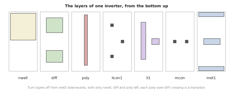
With only nwell, diff and poly left, the view stops looking like a tangle of wires and starts looking like what it is: transistors. Every place a poly strip crosses a diffusion rectangle is a gate, a physical transistor you can see rather than infer from a netlist.
This is what experienced layout engineers do first with an unfamiliar GDS, before running any automated checker. Building a visual sense of a layout comes before automating judgements about it.
One confusion to avoid: li1 and met1. SKY130 has the local interconnect layer li1 below met1, used heavily for wiring inside cells, and in some colour schemes the two look similar. Check the layer name, not just the colour, to tell them apart.
Practice Exercise
With only diff and poly visible, you look at a small region of one cell row. You count 6 poly strips, and each one crosses two separate diffusion regions: the NMOS diffusion in the lower half of the row and the PMOS diffusion in the upper half. Roughly how many transistors are in that region, and why is the answer not simply 6?
Solution
Each strip forms a gate wherever it crosses diffusion. A strip that crosses both the NMOS and the PMOS diffusion forms two transistors, one NMOS and one PMOS, sharing the same gate signal. So 6 strips give about 12 transistors, 6 CMOS pairs. The thing to count is crossings of poly over diffusion, not poly strips. A single piece of poly routinely forms both halves of a CMOS pair.
In the next article we use the layout to follow a single net and check that what we see matches what the netlist says.