From GDS to Mask to Wafer
In the previous article the GDS left your hands. In this article we follow what happens to it physically between “accepted for the shuttle” and “a wafer full of chips”.
Masks
A GDS file is a hierarchical database of polygons, each on a layer. Making the masks turns that idea into objects. The mask shop first prepares the data: it flattens the hierarchy, adds the fill and the alignment and test structures, applies corrections that pre-distort shapes so they print as intended, and combines drawn layers into the actual mask layers the process needs. Each mask layer then becomes a photomask, a quartz plate patterned with chrome: opaque or clear depending on whether the layer has geometry at that point. A process like SKY130 needs a few dozen masks, one for each patterning step: wells, implants, diffusion, poly, contacts, and every metal and via layer.
Building the wafer
The wafer is built by repeating one cycle for each mask, from the bottom of the stack to the top, as in Figure 1.
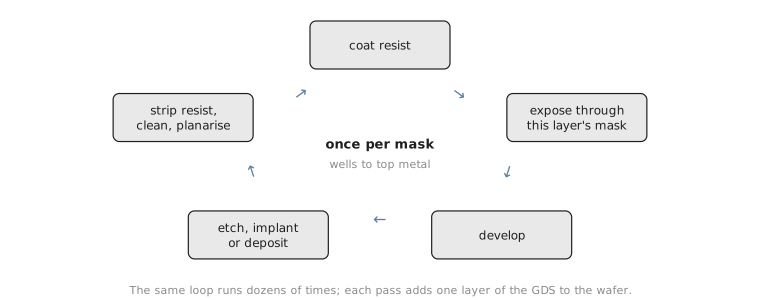
Coat the wafer with photoresist, expose it through the mask, develop it so the resist stays only where the pattern says, then etch, implant or deposit through the openings, and finally strip the resist, clean, and planarise where needed. Wells and diffusion come first, then poly, which forms a transistor gate wherever it crosses diffusion (the same crossings you found by eye in Section 9.2), then the contacts, then each metal and via layer in turn. It is the polygon database from Section 9.1 being turned into silicon, oxide and metal, one mask at a time.
Stepping the reticle across the wafer
The mask pattern does not cover a whole wafer. It covers one exposure field, the reticle field. On a shared shuttle the organiser arranges all the projects’ dies into one reticle layout, and the stepper exposes that pattern again and again in a grid across the wafer, producing many copies of every project.
You can estimate how many die fit in one field by simple division:
$$ N_{\text{slots}} \approx \left\lfloor \frac{W_{\text{field}}}{W_{\text{die}}} \right\rfloor \times \left\lfloor \frac{H_{\text{field}}}{H_{\text{die}}} \right\rfloor $$
As an illustration, a 3 mm × 4 mm die in a 26 mm × 33 mm field, which is the usual maximum field size of modern steppers:
$$ N_{\text{slots}} \approx \left\lfloor \frac{26}{3} \right\rfloor \times \left\lfloor \frac{33}{4} \right\rfloor = 8 \times 8 = 64 $$
This ignores the scribe lines between die, the saw streets where the wafer is cut, and any test structures the fab places in the field, so treat it as an order of magnitude, “tens”, not an exact count. Multiply by the number of fields on the wafer, minus the partial fields near the edge, and you have the die per wafer.
Real counts are always somewhat lower than the simple area division, because scribe lines and the unusable ring near the wafer’s edge take their share. This is also why “smaller die, more die per wafer, lower cost per chip” is one of the most basic cost relationships in the industry, going back to the die area discussion in Module 1.
Practice Exercise
If your die area doubled, say from 3 × 4 mm to about 4.2 × 5.7 mm, with the same field and wafer, would the number of die per wafer roughly halve? Why is the real answer usually worse than half?
Solution
By area alone it would roughly halve, since each die takes twice the space. In practice it is usually worse, for three reasons. The integer packing wastes more of the field with big die: here 26/4.2 and 33/5.7 give 6 × 5 = 30 slots, less than half of 64. More of each partial field at the wafer edge is lost, because a big die fits into fewer of the leftover spaces. And, as the next section explains, a bigger die is more likely to contain a random defect, so a smaller fraction of the fewer die you get will work.
In the next article we follow the wafer through dicing and packaging to the first power-on of the returned chip.